
Toshiba and Japan Semiconductor Develop Technology to Improve Reliability of Pch-LDMOS for Analog ICs
September 23, 2020
Toshiba Electronic Devices & Storage Corporation
Japan Semiconductor Corporation
TOKYO--Toshiba Electronic Devices & Storage Corporation (“Toshiba”) and its manufacturing subsidiary, Japan Semiconductor Corporation, have developed technology to improve the reliability of P-channel Laterally Double Diffused MOS (Pch-LDMOS) technology for analog ICs. The companies clarified the cause of degradation of breakdown voltage that occurs in the drain avalanche hot-carrier (DAHC) stress test, a reliability test for LDMOS, and identified a device structure that suppresses the degradation.
Details were reported at the IEEE-sponsored International Symposium on Power Semiconductor Devices and ICs 2020 (ISPSD 2020) held online.
The electrification of vehicles and automation of industrial equipment is stimulating demand for analog ICs that can maintain high reliability over the long term in low- and high-temperature environments. This has drawn increasing interest in LDMOS, which has low on-resistance that makes it suitable for a wide range of application.
In the drain avalanche hot-carrier (DAHC) stress test, LDMOS reliability is evaluated by applying a medium voltage to its gate over a long period. The test measures degradation of breakdown voltage, a known cause of damage and reduced reliability in analog ICs.
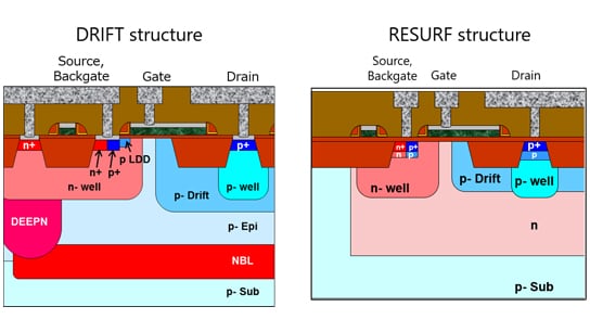
Until now, the mechanism that causes the degradation in breakdown voltage was not clear, but widely assumed to be due to a trapped charge in the corner of the shallow trench isolation (STI) [1], where the impact-ionization rate is the highest. The two companies’ investigation of electron flow and device structure found that the cause was different, a trapped charge in the bottom STI, not the corner.
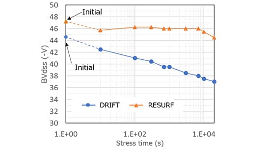
The companies found that the RESURF structure [2] is more tolerant of breakdown voltage degradation than the more commonly used DRIFT structure [3], because an additional junction underneath the drift region shares balances the total electric field across the region. The RESURF structure suppresses degradation to two-thirds that of the DRIFT structure. [4]
Cross sections of DRIFT and RESURF Pch-LDMOS structures
Improved reliability demonstrated by the DAHC stress test
Note
[1] STI: Shallow Trench Isolation. This divides elements or electrodes by embedding insulator film into shallow trenches.
[2] Comparison of breakdown voltage degradation in DAHC stress test after 5.5 hours. Breakdown voltage in the DRIFT structure falls 7.6V, but in the RESURF structure, it falls only 2.8V.
[3] DRIFT structure: an LDMOS structure in which the P-channel drift region is surrounded by the same P-channel region.
[4] RESURF structure: an LDMOS structure in which the P-channel drift region is surrounded by the N-channel region.
Customer Inquiries
System Devices Sales & Marketing Dept.
Sales Promotion Group
Tel: +81-3-3457-3332
* Information in this document, including product prices and specifications, content of services and contact information, is current on the date of the announcement but is subject to change without prior notice.
* Company names, product names and service names may be trademarks of their respective companies.