


在双极性输出与双扩散金属氧化物半导体(DMOS)输出之间实现低导通电阻
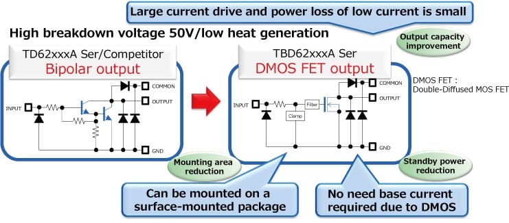
在输出阶段使用双扩散金属氧化物半导体(DMOS)场效应晶体管(FET),实现高效率和高输出电流。
自发明起,双极型晶体管40年来广泛用于各类应用。双极型晶体管需要大输入电流,因此有时需由辅助电路驱动双极型晶体管。
相较于双极型晶体管阵列,新型双扩散金属氧化物半导体(DMOS)场效应晶体管(FET)阵列所需的输入电流明显更低,因此更便于直接连接微控制器(MCU)。此外,DMOS FET晶体管阵列由于输入阶段的导通电阻减小,因此可承受更高的电压且耗电量更低。
- 与东芝先前的产品系列相比,这款产品的功率损耗大约降低了40%(Ta=25°C,输出电流=200mA)。
- 低输入电流:0.1mA(最大值)(输入电压=3V)
- 输出阶段的绝对最大额定值(TBD62064A与TBD62308A系列)
- 输出击穿电压:50V
- 输出电流(最大值):1.5A
- 输出击穿电压:50V
购买、样品、及IC可靠性查询
库存查询与购买
请输入3个以上字符
keyword:
Disclaimer for External Link
Through this website you are able to proceed to the website of our distributors ("Third Party Website") which is not under the control of Toshiba Corporation and its subsidiaries and affiliates (collectively "Toshiba"). The Third Party Website is made available to you as a convenience only and you agree to use the Third Party Website at your own risk. The link of the Third Party Website does not necessarily imply a recommendation or an endorsement by Toshiba of the Third Party Website. Please be aware that Toshiba is not responsible for any transaction done through the Third Party Website, and such transactions shall be subject to terms and conditions which may be provided in the Third Party Website.
Through this website you are able to proceed to the website of our distributors ("Third Party Website") which is not under the control of Toshiba Corporation and its subsidiaries and affiliates (collectively "Toshiba"). The Third Party Website is made available to you as a convenience only and you agree to use the Third Party Website at your own risk. The link of the Third Party Website does not necessarily imply a recommendation or an endorsement by Toshiba of the Third Party Website. Please be aware that Toshiba is not responsible for any transaction done through the Third Party Website, and such transactions shall be subject to terms and conditions which may be provided in the Third Party Website.
在新窗口打开