


MOSFET栅极驱动IC概述
东芝MOSFET栅极驱动器IC是一款用于外部N沟道MOSFET的开关控制器件,内置电荷泵和保护电路。它们采用超紧凑封装(1.2mm×0.8mm)、低静态电流和宽输入电压。将它们与N沟道MOSFET结合使用,该解决方案可实现小尺寸和低损耗的电源线。东芝可提供多种过电压锁定功能。

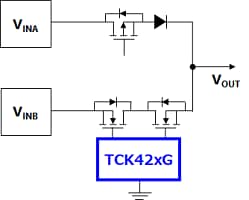

东芝MOSFET栅极驱动器IC可用于单高边、背对背负载开关和电源多路复用器。
东芝栅极驱动IC可与多种东芝N沟道MOSFET结合使用。东芝可提供模拟、开关评估和SOA(安全工作区)等各种技术数据的支持。
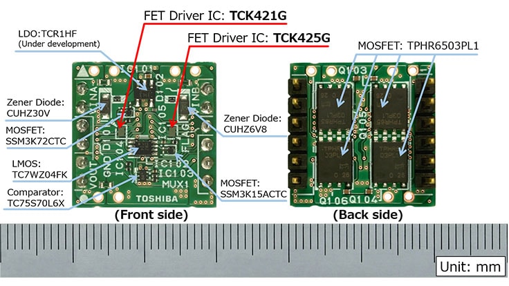
在一个小型PCB上实现具有2个输入和1个输出的电源多路复用器电路。
请访问并下载下方内容以获取更多详细信息
推荐产品列表
| 器件型号 | TCK401G | TCK402G | TCK420G | TCK421G | TCK422G | TCK423G | TCK424G | TCK425G |
|---|---|---|---|---|---|---|---|---|
| 数据表 | PDF(526KB) | PDF(3156KB) | ||||||
| 库存查询 |  |
|
|
|
|
|
|
|
| 最大输入电压 VIN最大值 |
40V | |||||||
| 输入电压范围 VIN |
2.7V至28V | |||||||
| 栅极驱动电压 VGATE |
4V至10V(VIN依从) | 10V | 5.6V | |||||
| 封装 | WCSP6E (1.2mm×0.8mm,厚度:0.55mm) |
WCSP6G (1.2mm×0.8mm,厚度:0.35mm) |
||||||
| 过压锁定阈值 | 28V | 27.73V | 23.26V | 14.29V | 10.83V | 6.31V | ||
| 欠压锁定阈值 | 2.7V | 2V | ||||||
| 使用方式 | 共源极 (可以单高边) |
共漏极 (可以单高边) |
||||||
相关信息
购买、样品、及IC可靠性查询
库存查询与购买
请输入3个以上字符
keyword:
Disclaimer for External Link
Through this website you are able to proceed to the website of our distributors ("Third Party Website") which is not under the control of Toshiba Corporation and its subsidiaries and affiliates (collectively "Toshiba"). The Third Party Website is made available to you as a convenience only and you agree to use the Third Party Website at your own risk. The link of the Third Party Website does not necessarily imply a recommendation or an endorsement by Toshiba of the Third Party Website. Please be aware that Toshiba is not responsible for any transaction done through the Third Party Website, and such transactions shall be subject to terms and conditions which may be provided in the Third Party Website.
Through this website you are able to proceed to the website of our distributors ("Third Party Website") which is not under the control of Toshiba Corporation and its subsidiaries and affiliates (collectively "Toshiba"). The Third Party Website is made available to you as a convenience only and you agree to use the Third Party Website at your own risk. The link of the Third Party Website does not necessarily imply a recommendation or an endorsement by Toshiba of the Third Party Website. Please be aware that Toshiba is not responsible for any transaction done through the Third Party Website, and such transactions shall be subject to terms and conditions which may be provided in the Third Party Website.
在新窗口打开