
Toshiba unveils 130nm Fit Fast Structured Array development platform
13th November 2018
Customers will benefit from high performance, low power consumption and lower costs
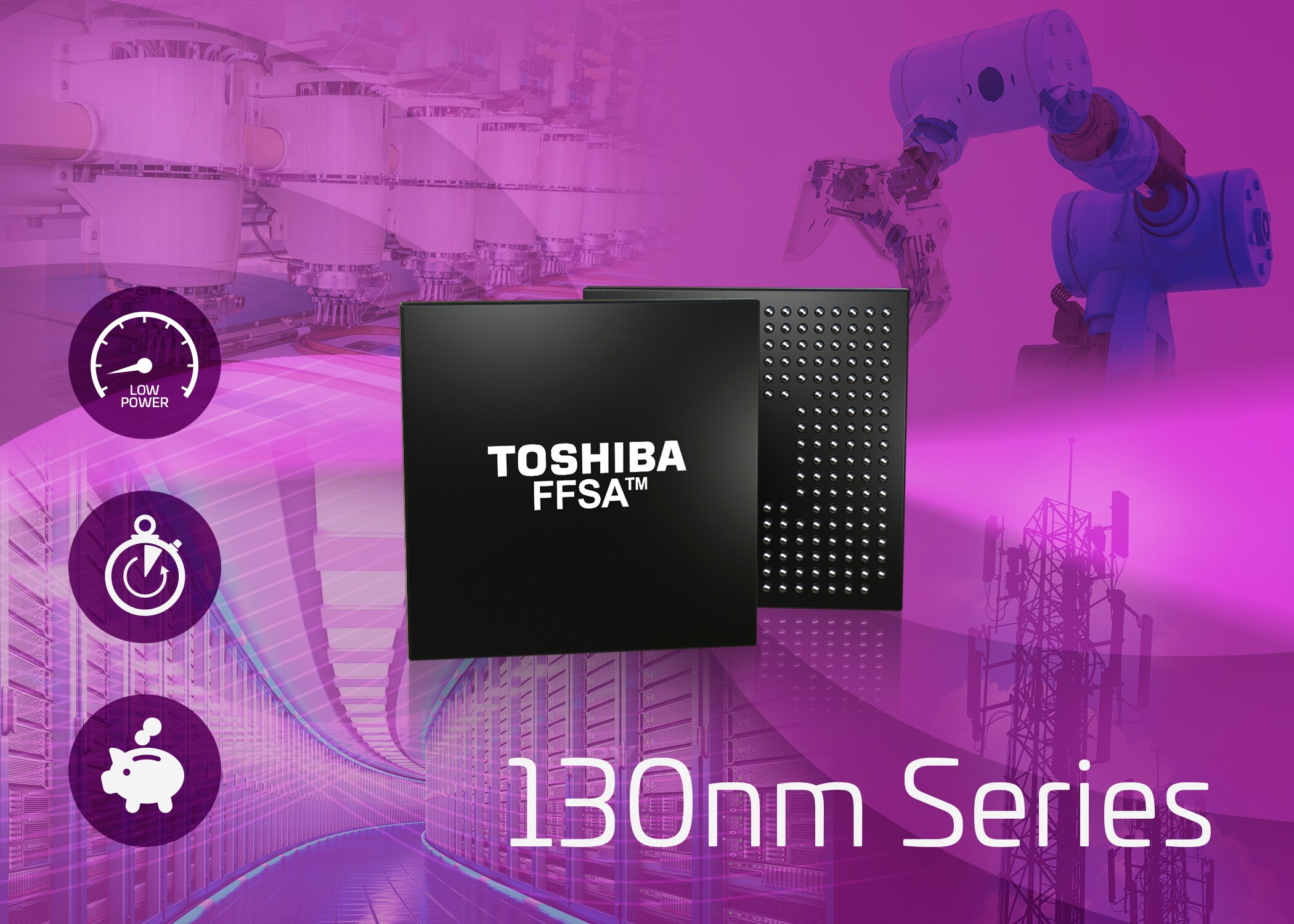
Toshiba Electronics Europe (“Toshiba”) today announced the very first customer shipment of a new 130nm manufacturing process node based FFSA™ (Fit Fast Structured Array) development platform. This innovative high performance System-on-Chip (SoC) development platform delivers custom solutions that feature low power consumption at a low cost point.
Toshiba provides ASIC (Application Specific IC) and FFSA™ platforms that suit the customer's business environment and technical requirements, that also deliver efficient solutions for custom SoC development. Using an innovative approach, all FFSA™ devices have a common silicon-based master layer that is used in combination with upper metal layers that are reserved and allow device customization.
The FFSA™ platform meets customer requirements for high performance and low power consumption; however, by limiting the customization to just the metal layer masks, it also reduces development cost drastically. As a result, samples and mass-produced devices can be delivered in a significantly shorter time than for conventional ASICs. Customers using the FFSA™ ASIC design methodology and library secure higher performance and lower power consumption than is possible with Field Programmable Gate Arrays (FPGAs).
The new FFSA™ 130nm process is added to Toshiba’s current 28, 40, and 65nm process portfolio adding another option for industrial equipment. The 130nm node process offer different master slices for up to 664kb of RAM and around 912,000 gates per device.
Devices designed on the platform will be manufactured by Japan Semiconductor, a subsidiary of Toshiba Electronic Devices & Storage Corporation with a long and proven track record of expertise in manufacturing ASIC, ASSP and microcomputers. This will ensure long-term supply continuity and meet or exceed the needs of customer business continuity plans.
Devices based on the new FFSA™ 130nm node process deliver the performance and integration needed for multiple application sectors including industrial equipment, communication technology, OA equipment and more.
Notes:
[1] The number of available gates is a guideline and will vary by application
* FFSA™ is a trademark of Toshiba Electronic Devices & Storage Corporation.
* All other company names, product names and service names may be trademarks of their respective companies.
Follow the link below for more information on the new development platform.
News Links


High Resolution Image (jpg)