
Toshiba and Japan Semiconductor Demonstrate Simultaneous Optimization of ESD Tolerance and Power Efficiency for High Voltage LDMOS for Automotive Analog ICs
June 11, 2021
Toshiba Electronic Devices & Storage Corporation
Japan Semiconductor Corporation
TOKYO--Toshiba Electronic Devices & Storage Corporation (“Toshiba”) and Japan Semiconductor Corporation (“Japan Semiconductor”) have together demonstrated a method for improving at the same time both the reliability and the performance of high voltage Laterally Double Diffused MOS (LDMOS), core components of analog ICs used in a wide range of automotive applications, such as motor control drivers. As the electrification of vehicles progresses, including wider deployment of advanced driver assistance systems (ADAS), Toshiba and Japan Semiconductor will be able to offer improved LDMOS cell design based on desired voltages.
Details of the achievement were reported at the IEEE-sponsored International Symposium on Power Semiconductor Devices and ICs 2021 (ISPSD 2021), held online.
There has been a trade-off in LDMOS design between reliability and performance. It is known that tolerance of electrostatic discharge (ESD), as measured using the human body model (HBM), is improved by increasing the backgate ratio*1 to suppress lateral parasitic bipolar action*2, which degrades HBM tolerance. However, increasing the backgate ratio also increases on-resistance, which degrades performance. Until now, LDMOS designers have had to balance HBM tolerance against higher on-resistance.
Toshiba and Japan Semiconductor evaluated HBM tolerance in LDMOS and found no increase at above 80V, even if the backgate ratio was increased. In a 2D TCAD simulation, they found that this is due to the appearance of vertical parasitic bipolar action alongside lateral parasitic bipolar action, a phenomenon that will give designers greater freedom when setting parameters for HBM and the backgate ratio.
Using this discovery in conjunction with a technology developed by Toshiba Corporation that optimizes cell design parameters other than the backgate ratio*3, Toshiba and Japan Semiconductor propose a method for improving HBM tolerance and suppressing on-resistance in 80V and higher LDMOS, which have HBM tolerance and no dependence on the backgate ratio. This can cover devices used in engines, steering and other automotive systems, and will contribute to improved reliability and power efficiency.
Toshiba has a wide lineup of LDMOS of various voltages for various applications, and is developing fifth generation process technology that will integrate embedded non-volatile memory (eNVM) and high voltage analog ICs.
Toshiba Electronic Devices & Storage Corporation and Japan Semiconductor Corporation are committed to semiconductor process R&D that contributes to low power consumption and high reliability.
Relationship between HBM tolerance and backgate ratio (Toshiba’s test results)

Difference of parasitic bipolar action undergoing HBM testing in low-voltage and high-voltage LDMOS (Toshiba’s test results)
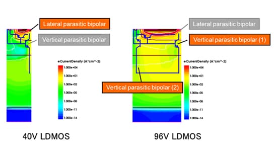
In low-voltage LDMOS, lateral parasitic bipolar action is dominant.
In high-voltage LDMOS, vertical parasitic bipolar action is dominant.
Notes
[1] Backgate ratio: Toshiba LDMOS have alternating sources and backgates along their width. Backgate ratio refers to the overall width of backgates against that of the sources and backgates.
[2] Parasitic bipolar action: A phenomenon observed during HBM tests; when positive voltage is applied to the LDMOS drain, impact-ionization occurs at the PN junction. The drain/body/source works as a collector/base/emitter of the parasitic bipolar transistor, and collector current flows. The collector current concentrates at the Si surface and lattice temperature increases, resulting in device destruction.
[3] Details of the technology were reported at ISPSD 2017. (Title: “HBM robustness optimization of fully isolated Nch-LDMOS for negative input voltage using unique index parameter.”)
Customer Inquiries:
*Company names, product names, and service names may be trademarks of their respective companies.
*Information in this document, including product prices and specifications, content of services and contact information, is current on the date of the announcement but is subject to change without prior notice.