


ΔΣ AD Converters
Toshiba's new microcontroller for designing smart meters has integrated high-accurate ΔΣ AD converters to precisely measure the power consumption. This article will explain the basics of AD conversion technique and the mechanism of the ΔΣ AD converter.
Smart Meter Usage
Recently saving energy is one of the most important issues in our daily life. Some developed countries intend to introduce smart grid systems and to supply most effectively their energy. The smart grid system requires smart meters which measure precise amount of used electric power and transfer the data with wireless means in real time. A new microcontroller has been developed which aims to give one-chip solution for designing the smart meters and integrates high-accurate ΔΣ AD Converters to measure the power consumption.
ΔΣ AD converters have been used in audio systems to reduce noise during
music data transfer. The system is called ‘1-bit Digital Audio’ system which is
now very popular.
Conventional AD Converters
Before introducing ΔΣ AD converters, conventional AD Converters will be explained.
There are variety types of AD converter for different applications.
Direct-conversion, successive-approximation, and integrating AD converters are popular and widely used. Brief explanations are given for each type of AD converters.
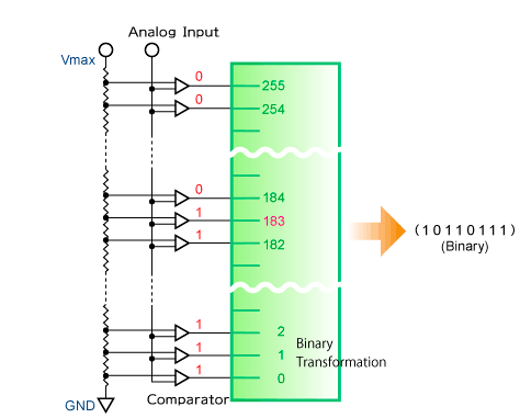
(1) Direct-conversion AD Converter
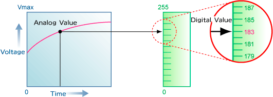
This type of AD converters converts an analog input signal to a digital data in one shot. It is just like measuring length. The conversion time is so short, short as one clock period. The drawbacks are large circuit area and power consumption.
The circuit configuration is as follows.
A circuit of series of many resistors is connected between the full-scale voltage Vmax and Ground, and a suitable number of terminals are set up on the string resistors at regular intervals. Each terminal goes to a comparator where the terminal voltage is compared with an analog input voltage. The comparator outputs high-level when the analog input voltage is larger than the terminal voltage, and it outputs low-level when the former is lower than the latter.
The comparator outputs, as a whole, are converted to Binary code.
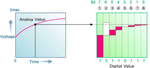
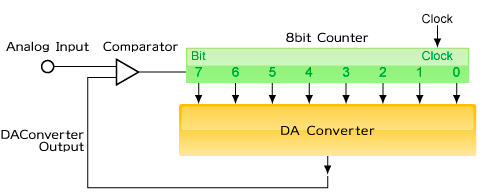
(2) Successive-approximation AD Converter
Successive-approximation type operates to generate analog voltage as a reference and to compare the reference voltage with an input analog voltage. The procedure is explained using 8bit AD converter of this type as an example. This type of AD converter employs a DA converter in it.
The DA converter performs reverse function of AD converters, converting a digital data to an analog data.
At first, the MSB (Most Significant Bit; Bit 7) is set to 1, and other 7 bits to 0. This means (10000000) in binary code. It goes to the DA converter and the converter generates the output voltage of half of Vmax. The output voltage is compared by a comparator with an analog input voltage. When the analog input is larger than the DA converter output, the MSB remains as 1. On the opposite when the analog input is smaller, the bit is reset to 0. In the case shown in the below figure, the analog input is larger than the DA converter output and the MSB stays as 1.
Next, the second MSB bit (Bit 6) is set to 1, which makes the binary code (11000000) in this case (the MSB is 1).
This code is input to the DA converter and the converter output is compared with the analog input. The result in this case is that Bit 6 is 0.
As the same manner comparison is done to each bit from higher significant bit. After all, digital data (10110111) remains in the 8-bit register. The value is the converted digital data of the input analog data.
The successive-approximation type is suitable to embedded AD converters in microcontrollers, because it has such good feature for small area and low power dissipation.

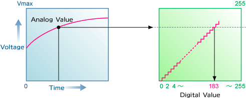
(3) Integrating AD Converter
One of the integrating-types counts how many steps are necessary to climb up from the bottom and to reach the level of an analog input voltage.
The converter circuit consists of a DA converter, a counter, and a comparator. Whenever the counter increments by a clock, the count value is converted to an analog value by the DA converter and the output is compared with an analog input voltage. The increment continues until the comparator detects the DA converter output is equal to or bigger than the analog input. When it happens, the converted digital value is in the counter.
This type should achieve higher accuracy potentially. The drawback is long conversion time.
Sampling and Quantization Noise
To convert analog signal to digital one, it is necessary to take a sample of analog signals. Even though ideally the sampled analog values will be converted precisely to corresponding digital values, the rest analog signal between neighboring sampled values is never converted. So the digital values have some errors for the original analog values. This error is called quantization error or quantization noise.
It is impossible to perform quantization noise-free conversion as long as sampling is necessary. Instead, how can the quantization noise be reduced? One of the easiest solutions is the higher frequency of sampling; the higher frequency, the less noise. The conversion time will, however, be too short to convert analog to digital at very high frequency.
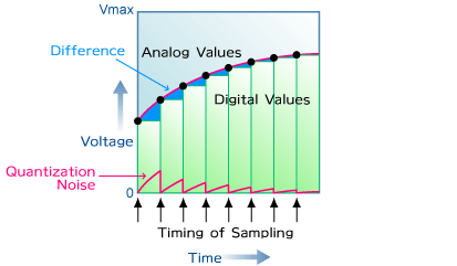
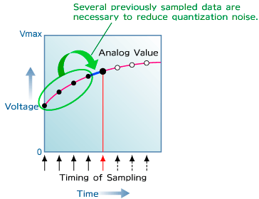
The analog signal between the neighboring sampled values is smoothly changing. If the smoothly sweep line needs to be re-created, several sampled data prior to the current sampled have to be taken in for the calculation.
ΔΣ AD converters perform high accuracy conversion by editing sampled data in very sophisticated method to reduce drastically quantization noise.
Now, we introduce ΔΣ AD converters.
Δ (delta) means subtraction, Σ (sigma) means addition (or integration). The converter operation is, firstly,
subtracting a reference value from input analog value, and,
secondly, adding the difference of the subtraction (integrated).
Though actual circuits are so complicated, the simplest model is introduced here.
ΔΣ AD Converter
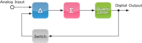
(1)Circuit Configuration
ΔΣ AD converters convert an analog signal to digital using ΔΣ modulation methodology. The ΔΣ modulation unit consists of four function blocks. Those are a Δ (subtraction) circuit which subtracts a certain value from input analog value, a Σ (addition or integration) circuit which adds the output values from the Δ circuit in sequence, a quantization circuit which compares the output value of the Σ circuit with a reference voltage and outputs digital value 1 or 0 depending on the magnitude of the Σ circuit, and a switch circuit whose output is selected by the output of the quantization circuit and goes to the Δ circuit.
(2) Function of ΔΣ Modulation
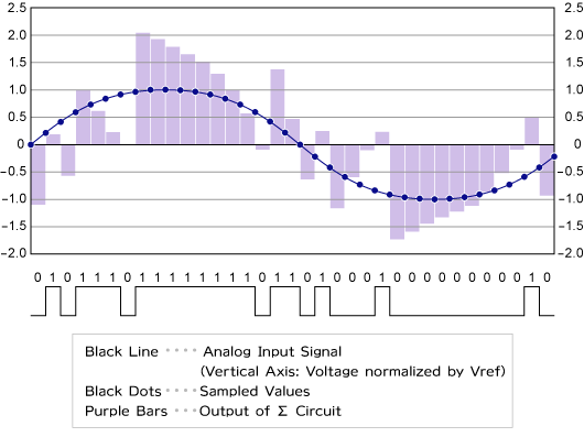
The function of ΔΣ modulation is explained on the above chart.
・An analog value Va enters the Δ circuit. Another input of the Δ circuit is Vo which is the output of the switch circuit. The value of Vo is either Vref or -Vref, and this case the initial value is assumed Vref. Then, the calculation result in the Δ circuit becomes Va-Vref (=Δ). Actually the Δ is a minas value because Vref is the maximum value of the input signal, and it goes to the Σ circuit.
・Supposing the initial output value of the Σ circuit is 0V, the addition result is
0+Δ = Δ.
・This value is transferred to the quantization circuit. Here the reference voltage is assumed 0V. The quantization circuit compares the input (the output of the Σ circuit) with the reference voltage, and when the input is larger than the reference it outputs 1 and when the input is smaller, 0. This case, the value Δ is negative. So the output of the quantization circuit is 0. This is the end of the operation in one clock period.
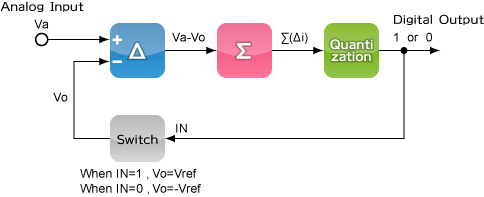
At the beginning of the next clock the switch circuit generates -Vref as Vo because the output of the quantization was 0 at the end of the previous clock.
Current analog value Va’ makes the output value of the Δ circuit Va’-(-Vref)=Va’+Vref (=Δ’). And the output of the Σ circuit results in Δ+Δ’. If this value is larger than 0V (the value is positive), the quantization circuit output is 1. On the contrary, if it is smaller, the output is 0.
As explained above, the operation sequence of subtraction, addition and comparison (quantization) makes a series of digital data which consist of either 1 or 0. The original analog signal can be recovered by the frequency of the appearance of 1 or 0 of the serial digital data with very small quantization noises.
One of the remarkable features of ΔΣ modulation is shown at the output of the Σ circuit. In the chart the Σ circuit output (bar graphs) changes rapidly compared with the smooth analog input signal. The bars are bobbing around the 0V crossing point of the input signal, while the bar once jumps to highest level around the top area and gradually decreases later, and around the bottom, vice versa.
Though the Σ circuit output is quite different from the input analog signal, it contains the information of the magnitude and the changing tendency of the latter signal.
Umm…., it is not easy.
But looking at the serial digital data, you can imagine the
shape of the input analog signal, can’t you?
That is, continuous 1s implies some hill shape,
continuous 0, a valley, and the alternation of the data, 1 and 0,
indicates a slope, I guess.
High accuracy technology
We explained the operating principle using the simplest model. The real device has more sophisticated technology to perform high accuracy in ΔΣ AD converters.
The sampling frequency should be higher. Generally the higher frequency makes the less quantization noises for an AD converter, which is the same in the case of a ΔΣ AD converter.
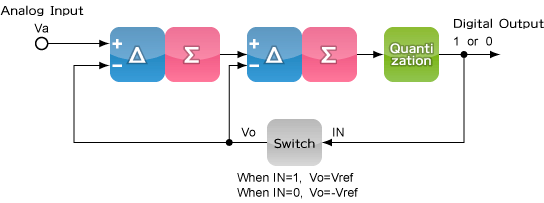
As explained, Δ and Σ process reduces quantization noises dramatically and more than one ΔΣ would provide the AD converter with more accuracy. Tow stage of ΔΣ process is called two-order ΔΣ modulation. It is common to build four stages, four-order ΔΣ modulation, in a real device of a ΔΣ AD converter.
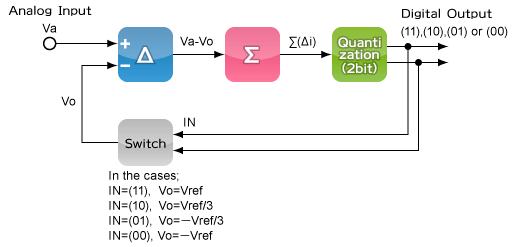
Another way to realize higher accuracy is to increase quantizing bits. So far, one bit quantization has been explained. Supposing the quantization bits become two, the output of the quantization circuit will be one of 2bit data, (11), (10), (01), and (00). The switch circuit will select one of four voltages, Vref, Vref/3, -Vref/3, and –Vref, accordingly. This also improves greatly the conversion accuracy, and more bits, more accurate.
Well…
A very unique conversion method is used in a ΔΣ AD converter to improve the performance.
I hope you have understood it well.