
A TVS diode with an increased peak pulse current rating to improve surge protection performance for mobile devices: DF2B5BSL
Product News 2018-12
Toshiba Electronic Devices & Storage Corporation ("Toshiba") has launched the standard capacitance TVS diode (ESD protection diode) “DF2B5BSL” that has increased its peak pulse current rating to improve surge protection performance.
The new product features a peak pulse current rating of 8 A[1], about 45 % increase from the existing product[2] to improve the protection performance against lightning surges complying with IEC61000-4-5. In addition, its electrostatic discharge voltage rating is ±23 kV[3], about 35 % increase from the existing product[2]. With these features against surge protection by improved performances, this new product contributes to improving the reliability of equipment.
Internal circuits of mobile devices such as smartphones and tablets are becoming more highly integrated to make these devices smaller and slimmer. ICs used in these devices are increasingly miniaturized in their manufacturing processes, yet the ICs are becoming less tolerant to ESD and surges. To prevent equipment from malfunctioning or breaking down due to ESD or surges, TVS diodes are often used to protect external terminals (such as power supply connectors, audio jacks) or ICs vulnerable to ESD.
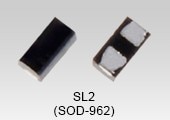
The new product uses the small SL2 package (package code: SOD-962). This makes its footprint on boards smaller, allowing it to be used for various applications.
Notes:
[1] According to IEC61000-4-5
[2] Existing product: DF2B5SL
[3] According to IEC61000-4-2 (Contact)
Features
- High peak pulse current rating[1]: IPP=8 A
- High electrostatic discharge voltage rating[3]: VESD= ±23 kV
- Low clamping voltage[4]: VC=9.6 V (typ.) @IPP=8 A
Notes:
[4] Based on IEC61000-4-5 8/20 μs pulse.
Applications
- Smart phones
- Tablets
- Game consoles, etc.
Product Specifications
(@Ta=25 °C)
| Part number |
Package | Absolute maximum ratings |
Working peak reverse voltage VRWM max (V) |
Reverse breakdown voltage VBR min/max @IBR=1 mA (V) |
Clamp voltage VC[4] typ. @IPP=8 A (V) |
Dynamic resistance RDYN[5] typ. @IPP1=8 A to IPP2=16 A (Ω) |
Total capacitance Ct typ. @VR=0 V (pF) |
||
|---|---|---|---|---|---|---|---|---|---|
| Name | Size typ. (mm) |
Electrostatic discharge voltage VESD[3] (kV) |
Peak pulse current IPP[1] (A) |
||||||
| SL2 (SOD-962) |
0.62×0.32×0.3 | ±23 | 8 | 3.3 | 3.6/6.5 | 9.6 | 0.2 | 10.5 | |
Notes:
[5] @TLP parameters: Z0=50 Ω, tp=100 ns, tr=300 ps, averaging window: t1=30 ns to t2=60 ns
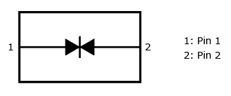
Internal Circuit
Application Circuit Example
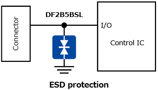
The application circuits shown in this document are provided for reference purposes only. Thorough evaluation is required, especially at the mass-production design stage. Toshiba Electronic Devices & Storage Corporation does not grant any license to any industrial property rights by providing these examples of application circuits.
Characteristic Curves
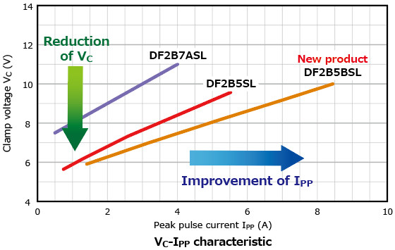
The new product has improved its protection performance against surges by increasing IPP.
In addition, with its reduced VC, it can reduce the impact on circuits in later stages.
Information in this document, including product prices and specifications, content of services and contact information, is correct on the date of the announcement but is subject to change without prior notice.