Low capacitance TVS diodes for automotive applications offering fine protection performance while keeping signal quality at several Gbps : DF2S5M4FS, DF2S6M4FS
Product News 2019-09

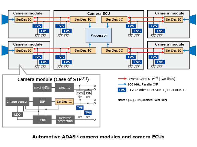
Toshiba Electronic Devices & Storage Corporation ("Toshiba") has launched two unidirectional, low capacitance TVS diodes, "DF2S5M4FS" (VRWM max=3.6 V) and "DF2S6M4FS" (VRWM max=5.5 V), which protect I/O ports of SerDes ICs[1] used for video signal lines of such as automotive ADAS[2] camera modules and ADAS[2] ECUs from noise and surges.
For automobiles, requirements for their safety functions are becoming stricter than ever together with the move toward automated driving. Improvement of camera’s performances (high image quality and resolutions) increase the amount of information, and the transfer of information to driving systems is shifting toward real-time communications. Therefore, high-speed LVDS[3] communications are increasingly used.
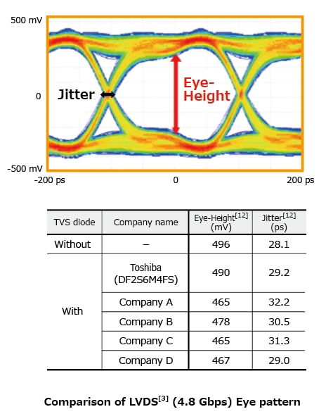
The new products DF2S5M4FS and DF2S6M4FS feature a maximum diode capacitance of 0.55 pF to handle high speed communications at several Gbps and it also keeps signal quality (eye patterns). In addition, by using our latest original process EAP-IV[4], they feature a typical clamp voltage of 7.5 V[5] and an electrostatic discharge voltage of ±30 kV[6] to prevent device breakdowns and malfunctioning to help increase system reliability.
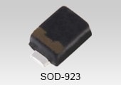
They use the industry standard SOD-923 (1.0×0.6 mm typ.) small size surface mounting package, which is suitable for downsizing of equipment. In addition, by conforming to AEC-Q101, they can be widely used for various automotive applications such as IVI[7] and electronic mirrors.
Notes :
[1] SerDes IC (Serializer/Deserializer IC : a picture signal IC to convert parallel data to serial data and vice-versa)
[2] ADAS (Advanced Driver Assistance System)
[3] LVDS (Low Voltage Differential Signaling, Transmission speed : Several Gbps)
[4] EAP-IV : Fourth generation ESD Array Process
[5] DF2S6M4FS
[6] According to ISO10605
[7] IVI (In-Vehicle Infotainment)
Features
- AEC-Q101 qualified
- Signal quality is kept by low capacitance at the time of the high-speed communication of several Gbps :
Ct=0.55 pF (max) - Low clamp voltage : VC=7.5 V (typ.) (DF2S6M4FS)
Applications
- Automotive ADAS[2] camera and IVI[7], etc.
Product Specifications
(@Ta=25 °C)
| Part number | ||||
|---|---|---|---|---|
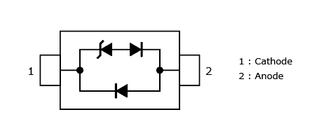
| Configuration | Unidirectional | |||
| Package | SOD-923 | |||
| Absolute maximum ratings |
Electrostatic discharge voltage VESD (kV) |
@Contact[8] | ±20 | ±20 |
| @Air[8] | ±20 | ±20 | ||
| @Contact[6] | ±30 | ±30 | ||
| @Air[6] | ±30 | ±30 | ||
| Peak pulse power PPK (W) | @tp=8/20 μs | 30 | 30 | |
| Peak pulse current IPP (A) | 2 | 2 | ||
| Recommended operation conditions |
Working peak reverse voltage VRWM max (V) | 3.6 | 5.5 | |
| Electrical characteristics |
Reverse breakdown voltage VBR min (V) | @IR=1 mA | 3.7 | 5.6 |
| Reverse breakdown voltage VBR max (V) | 5.5 | 7.9 | ||
| Reverse current IR max (μA) | @VRWM max | 0.1 | 0.1 | |
| Clamp voltage VC typ.[9] (V) | @IPP=1 A | 6.8 | 7.5 | |
| Dynamic resistance RDYN typ.[10] (Ω) |
0.35 | 0.35 | ||
| Total capacitance Ct max (pF) | @VR=0 V, f=1 MHz | 0.55 | 0.55 | |
Notes :
[8] According to IEC61000-4-2
[9] According to IEC61000-4-5
[10] TLP parameter: Z0=50 Ω, tp=100 ns, tr=300 ps, averaging window t1=30 ns to t2=60 ns,
extraction of dynamic resistance using least squares fit of TLP characteristics between IPP1=8 A and IPP2=16 A.
Equivalent Circuit

Application Circuit Example

The application circuits shown in this document are provided for reference purposes only.
Thorough evaluation is required, especially at the mass production design stage.
Providing these application circuit examples does not grant any license for industrial property rights.
Characteristic Curves (Reference)

Notes :
[12] As of May 2019, values measured by Toshiba
Information in this document, including product prices and specifications, content of services and contact information, is correct on the date of the announcement but is subject to change without prior notice.