Lineup expansion of 100 V N-channel power MOSFET U-MOSIX-H series products that help improve the efficiency of power supplies: TK2R9E10PL, etc.
March 23, 2018
Toshiba Electronic Devices & Storage Corporation

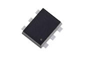
TOKYO--Toshiba Electronic Devices & Storage Corporation (“Toshiba”) has released a dual MOSFET “SSM6N813R” with high ESD protection positioned for use in automotive applications, including as a driver IC for headlight LEDs, which require a high withstand voltage and a small footprint. Mass production shipments begin in April.
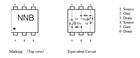
A maximum drain-source voltage (VDSS) of 100V ensures that SSM6N813R is suitable for headlight applications requiring multiple LEDs—a capability supported by high ESD immunity. Fabricated using the latest process and housed in a TSOP6F package, SSM6N813R has an allowable power dissipation of 1.5W and low on-resistance. In addition, the footprint of the TSOP6F package is 70% smaller than that of an SOP8 package.
Applications
- Automotive headlight LED driver
Features
- Small package
- High ESD protection
- Low RDS(ON)
Main Specifications
(@Ta=25℃)
Items |
SSM6N813R | ||
|---|---|---|---|
| Absolute maximum ratings | Drain-source voltage VDSS (V) |
100 | |
| Gate-source voltage VGSS (V) |
±20 | ||
| Drain current ID (A) |
3.5 | ||
| Electrical Characteristics | Drain-source on-resistance RDS(ON) max (mΩ) |
VGS=10V | 112 |
| VGS=4.5V | 154 | ||
| Input capacitance Ciss typ. (pF) |
242 | ||
| Package | 2.9mm×2.8mm; t=0.8mm | ||

Customer Inquiries:
Small Signal Device Sales & Marketing Department
Tel: +81-3-3457-3411
Information in this document, including product prices and specifications, content of services and contact information, is current on the date of the announcement but is subject to change without prior notice.