Analog Power IC Process Technology Developed by Toshiba and Japan Semiconductor Enhances Reliability of LDMOS for Automotive Applications
May 30, 2019
Toshiba Electronic Devices & Storage Corporation
Japan Semiconductor Corporation
TOKYO -- Toshiba Electronic Devices & Storage Corporation (Toshiba) and its manufacturing subsidiary, Japan Semiconductor Corporation, have developed process technology for N-channel Lateral Double Diffused MOS (LDMOS) for 0.13-micron generation analog power ICs that ensures high reliability, even at the high temperatures of automotive applications. The technology cuts leak current from crystal defects, and boosts the lifetime [1] of LDMOS in high temperature environments (175°C) to ten times [2] that of Toshiba’s current technology.
Details were reported on May 22 at the IEEE-sponsored International Symposium on Power Semiconductor Devices and ICs 2019 (ISPSD 2019) in Shanghai.
Demand of automotive semiconductors is increasing with the electrification of vehicles. Devices used must be able to maintain high level reliability over the long term in a high temperature environment, which is driving interest in N-channel LDMOS, now mainly used in motor control ICs for industrial equipment and consumer electronics.
In LDMOS manufacturing, high-dose ion implantation degrades the crystalline structure of the silicon layer. Higher doses result in more degradation, and increase the undesirable impact on performance characteristics. This results in two significant problems for LDMOS: the larger the area, the more the initial leak current failure; and long-term use in hot environments, such as automotive applications, causes high temperature reverse bias (HTRB) degradation, and drastic increases in leak current.
Toshiba and Japan Semiconductor Corporation found solutions by combining Toshiba’s know-how in transistor design with Japan Semiconductor’s process technologies.
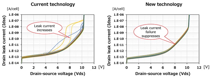
Initial leak current failure due to crystal defects during the manufacturing process was solved by changing the STI [3] filling material used for LDMOS. Currently, HDP-CVD [4] is used to fill STI on the edge of LDMOS, but replacing it with SA-CVD [5] imposes less stress on the silicon. With SA-CVD, no chip failure due to leak current was found, because there was no damage to the silicon’s crystalline structure, even during high-dose ion implantation. This confirmed the ability of the new technology to suppress initial leak current failure.
The companies identified the cause of HTRB degradation by analyzing its mechanism, and found that the edge design of LDMOS is key; high-dose implantation near the STI/Si edge resulted in crystal defects in the silicon. While the annealing process, the dangling bond of the silicon is connected by proton that temporarily hides them, the protons de-connected from the dangling bond during HTRB stress, and current leakage due to crystal defects increases.
The companies changed the LDMOS layout to keep the high-dose implanted area away from the highly stressed area close to the STI, and covered the STI/Si interface with gate poly silicon which is used for the gate electrodes in LDMOS. This suppresses the value of the critical stress of the area near the STI, where the high stress exists, and reduces HTRB degradation.
The companies will start mass production of analog ICs for automotive application with the new process technology from July this year.
Toshiba has wide range of lineup of LDMOS for various voltages and applications, and also develops fourth generation LDMOS to decrease on‐resistance half compares to Toshiba’s current devices.
Toshiba Electronic Devices & Storage Corporation and Japan Semiconductor Corporation are committed to semiconductor process R&D that contributes to low power consumption and minimized equipment size.
Notes
[1]Defined by the companies as “the period between the initial status and the time when leak current reaches its upper limit.”
[2] Compared to Toshiba’s current LDMOS for consumer electronics
[3] STI: Shallow Trench Isolation. This separates elements or electrodes by embedding insulator film into shallow trenches.
[4] HDP-CVD: High Density Plasma assisted Chemical Vapor Deposition.
[5] SA-CVD: Sub-atmospheric Pressure Chemical Vapor Deposition.
Improvement of initial leak current failure

Improvement of HTRB degradation

* Company names, product names, and service names may be trademarks of their respective companies.
Information in this document, including product prices and specifications, content of services and contact information, is current on the date of the announcement but is subject to change without prior notice.