

Toshiba-Developed Technology Achieves both Higher Efficiency and Long-Term Reliability in Trench-Gate SiC MOSFETs
September 30, 2026
Toshiba Electronic Devices & Storage Corporation
Kawasaki, Japan-Toshiba Electronic Devices & Storage Corporation ("Toshiba") has developed a technology that suppresses threshold voltage (Vth)[1] drift during long-term operation in trench-gate silicon carbide (SiC) MOSFETs[2], a type of power semiconductor device, contributing to improved device reliability. By analyzing the relationship between gate oxide[3] interface treatment conditions and Vth drift and implementing an appropriate gate formation process, Toshiba suppressed the impact of charge traps[4] that contribute to the drift and reduced it by approximately 50% that of commercially available trench-gate SiC MOSFETs. Users require trench-gate SiC MOSFETs that lower power loss. The new technology contributes to higher efficiency and long-term reliability, and will help to improve reliability and energy efficiency in power conversion applications such as electric vehicles, renewable energy systems, and data center power supplies. Details of the technology were presented at the 23rd International Conference on Silicon Carbide and Related Materials (ICSCRM 2026), which is being held in Yokohama, Kanagawa, Japan, from September 27 to October 2, 2026.
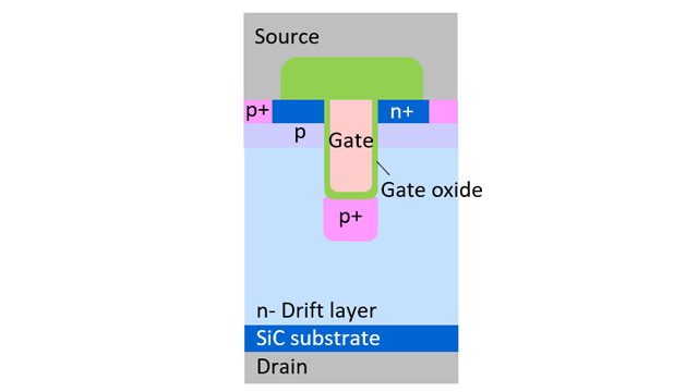
SiC MOSFETs, next-generation power semiconductors that deliver higher power conversion efficiency than silicon (Si) MOSFETs, are finding wider adoption in electric vehicles. Trench-gate SiC MOSFETs (Figure 1), which employ a trench-gate structure, feature low on-resistance[5] and high current density and are expected to further lower power loss.
However, they also experience greater Vth drift from prolonged application of voltage stress[6] than Si MOSFETs. Vth drift occurs when a positive or negative voltage is constantly applied to the gate electrode. It is recognized as a major reliability concern. Recent years have also seen reports of variations in Vth depending on the number of stress cycles[7] when positive and negative voltages are repeatedly applied to the gate electrode ("positive/negative stress"). Such Vth drift can affect stable MOSFET operation and lead to increased conduction loss[8], and is an important issue from the perspective of long-term reliability. This issue is particularly pronounced in some trench-gate SiC MOSFETs, creating a challenge that must be addressed in order to achieve high efficiency and high reliability.
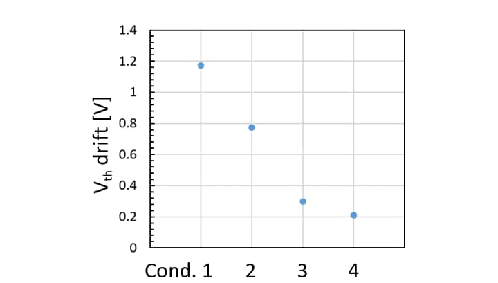
Toshiba addressed the problem by focusing on the interface treatment applied during formation of the gate oxide in the trench region. Such treatment has conventionally been used to reduce on-resistance and improve gate oxide reliability; however, its impact on Vth drift in environments of repeated application of positive and negative stress were insufficiently investigated or understood. Evaluation results confirmed that Vth drift magnitude varies significantly after applying positive/negative stress to the gate electrode, depending on nitridation conditions and other interface treatment parameters (Figure 2). Further analysis suggested that charge traps generated during the interface treatment contributed to the drift. Toshiba used these findings to optimize gate oxide interface treatment conditions and other process parameters and established a gate formation process that suppresses Vth drift caused by positive/negative stress while maintaining low on-resistance.
Using the new technology, Toshiba reduced Vth drift to approximately 50% that of commercially available trench-gate SiC MOSFETs (Figure 3), demonstrating its effectiveness in significantly suppressing one of the key issues with SiC trench MOSFETs and contributing to improved long-term device reliability.
The technology has been applied to Toshiba's 1200V trench-gate SiC MOSFET "TW007D120E," which began test sample shipments in May 2026. Going forward, Toshiba will expand its application to other SiC MOSFETs and continue to promote higher reliability and higher efficiency in SiC power devices for automotive applications such as electric vehicles, and industrial applications, including renewable energy systems and data center power supplies.
This work is based on results obtained from a project, JPNP21029, subsidized by the New Energy and Industrial Technology Development Organization (NEDO).
![Figure 3. Comparison of V<sub>th</sub> drift between Toshiba's 1200V trench-gate SiC MOSFET and commercially available trench-gate SiC MOSFETs (Measurement conditions: 25°C, V<sub>gs</sub>=+25V/-10V, Duty<sup>[9]</sup> =50%, 400kHz, at 10<sup>11</sup> cycles. As of September 30, 2026, Toshiba test results)](/content/dam/toshiba-ss-v3/master/en/company/news/news-release/sic-power-devices/sic-power-devices-20260930-1_4_en.png)
Notes:
[1] Threshold voltage (Vth): The voltage required to turn on a MOSFET.
[2] MOSFET: Metal Oxide Semiconductor Field Effect Transistor, a switching device with three electrodes: gate, drain, and source. Current between the drain and source is switched on and off by applying a gate voltage.
[3] Gate oxide: A thin oxide film that separates the gate electrode from the semiconductor.
[4] Charge trap: A microscopic defect capable of capturing charge carriers.
[5] On-resistance: The resistance between the drain and source when a MOSFET is in operation.
[6] Voltage stress: Electrical stress imposed on a device by applying a voltage.
[7] Number of cycles: The cumulative number of switching cycles between positive and negative voltages applied to the gate electrode.
[8] Conduction loss: Power loss generated when current flows through a device in the on-state, mainly due to on-resistance.
[9] Duty: The proportion of positive-voltage application time within one cycle.
* Company names, product names, and service names may be trademarks of their respective companies.
* Information in this document, including product prices and specifications, content of services and contact information, is current on the date of the announcement but is subject to change without prior notice.