Toshiba’s New SiC MOSFETs Delivers Low On-Resistance and Significantly Reduced Switching Loss
July 22, 2022
Toshiba Electronic Devices & Storage Corporation
KAWASAKI--Toshiba Electronic Devices & Storage Corporation (“Toshiba”) has developed silicon carbide (SiC) MOSFETs[1] with low on-resistance and significantly reduced switching loss—about 20% lower than in its second-generation SiC MOSFETs.
Power devices are essential components for managing and reducing power consumption in all kinds of electronic equipment, and for achieving a carbon neutral society. SiC is widely seen as the next generation material for power devices, as it delivers higher voltages and lower losses than silicon. While SiC power devices are now mainly utilized in inverters for trains, wider application is on the horizon, in vehicle electrification and the miniaturization of industrial equipment. However, the adoption and market growth of SiC devices have been held back by reliability issues.
Toshiba has solved this problem by adopting a structure in which a Schottky Barrier Diode (SBD) is placed in parallel with the PN diode inside the SiC MOSFET of the second-generation product. However, this created a new problem, whereby the performance of the MOSFET deteriorates when it includes an SBD cell that does not operate as a MOSFET. Specifically, there is an increase in the on-resistance per unit area (RonA) and in the performance index that indicates the on-resistance and high speed (Ron*Qgd). A further problem was a higher unit cost from increasing the chip area to reduce on-resistance (Ron).
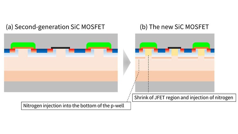
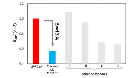
Toshiba has now developed a device structure that reduces RonA while including an SBD. Spread resistance (Rspread)[2] is reduced and the SBD current is increased by injecting nitrogen into the bottom of the wide p-type diffusion region (p-well) of the SiC MOSFET. Toshiba also reduced the JFET[3] region and injected nitrogen to reduce feedback capacitance and JFET resistance. As a result, feedback capacitance was reduced without increasing RonA. Toshiba prototyped and confirmed that this device structure reduces RonA by 43%[4], Ron*Qgd by 80%[5], and switching loss (from switching on and off) by about 20%[6], compared to its second-generation products. Stable operation without fluctuation of RonA was also secured by optimized positioning of the SBD.
Details of the achievement were reported at the PCIM Europe 2022, an international conference of power devices held in Nuremberg, Germany and online on May 12. Toshiba plans to start mass production of third generation SiC MOSFETs with the new technology in late August this year.
[1] MOSFET: metal-oxide-semiconductor field-effect transistor
[2] Spread resistance: The diffusion resistance at the bottom of the p-well.
[3] JFET: Junction Field Effect Transistor
[4] Comparison of the new 1.2kV SiC MOSFET when RonA is set to 1 in the second-generation SiC MOSFET. (Toshiba test results)
[5] Comparison of the new 1.2kV SiC MOSFET when Ron*Qgd is set to 1 in the second-generation SiC MOSFET. (Toshiba test results)
[6] Comparison of the new 1.2kV SiC MOSFET and the second-generation SiC MOSFET. (Toshiba test results)
The structure of Toshiba’s new SiC MOSFET

Reduction of RonA and Ron*Qgd (Toshiba test results)


*Company names, product names, and service names may be trademarks of their respective companies.
*Information in this document, including product prices and specifications, content of services and contact information, is current on the date of the announcement but is subject to change without prior notice.