Smart Gate Driver Photocoupler with 2.5 A Output Current Whose Output Type is Widely Used in Industrial Equipment
Product News 2022-05

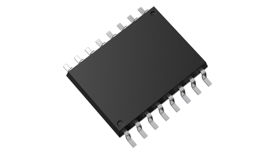
Toshiba Electronic Devices & Storage Corporation ("Toshiba") has launched a 2.5 A output smart gate driver photocoupler, TLP5212, that protects power devices from over-current which may be generated in circuits such as inverters that use medium-capacity IGBTs or power MOSFETs.
The new product has changed its output type from the current products[1] to meet specifications widely used in applications such as industrial equipment. In addition, the product has incorporated protection functions such as IGBT desaturation detection, active Miller clamp, and FAULT output, allowing the reduction of external circuits. This helps reduce the system costs for fault detection and protective operation. In addition, by incorporating Toshiba’s own highly reliable and high output power infrared LED, it can be used in a wide range of applications, including home photovoltaic power systems and industrial equipment such as UPSs[2] used in severe thermal environments.
With its propagation delay time and propagation delay skew specified at the operating temperature rating (Ta =-40 °C to 110 °C), this product allows easier design.
Its package, SO16L, is slim with a maximum height of 2.3 mm, helping improve the freedom in the layout of parts on a system board. In addition, it features a minimum creepage distance of 8 mm, allowing it to be used for applications requiring high insulation performance.
TLP5212 resumes stand-by mode from protective action by input side LED signal. TLP5222[3], which resumes to stand-by mode automatically after specified time, is under planning for mass production.
Notes :
[1] TLP5214 and TLP5214A
[2] UPSs : Uninterruptible power supplies
[3] Mass production is planned to start in July, 2022 (as of April 2022).
Applications
- Industrial equipment
Industrial inverters, AC servo drives, PV inverters, UPSs[2], etc.
Features
- Totem pole output circuit widely used in industrial equipment with two N-channel MOSFETs[4].
- Incorporated protection functions such as IGBT desaturation detection, active Miller clamp, and FAULT output.
- Peak output current rating : IOP=±2.5 A
Notes :
[4] They are an N-channel MOSFET for a source current and an N-channel MOSFET for a sink current.
Main Specifications
(Unless otherwise specified, @Ta=-40 °C to 110 °C)
Part number |
|||
|---|---|---|---|
Package |
Name |
SO16L |
|
Size (mm) |
10.3 × 10 (typ.) t : 2.3 (max) |
||
Absolute maximum ratings |
Operating temperature range Topr (°C) |
-40 to 110 |
|
Peak output current IOPH/IOPL (A) |
±2.5 |
||
Recommended operating conditions |
Total output side supply voltage (VCC2 - VEE) (V) |
15 to 30 |
|
FAULT feedback IC supply voltage VCC1 (V) |
2.7 to 5.5 |
||
Electrical characteristics |
Supply current Icc2H, Icc2L max (mA) |
5 |
|
Threshold input current (L/H) IFLH max (mA) |
6 |
||
DESAT threshold voltage VDESAT typ. (V) |
6.6 |
||
Switching characteristics |
Propagation delay time tpHL, tpLH max (ns) |
250 |
|
Propagation delay skew (device to device) tpsk (ns) |
-150 to 150 |
||
Common mode transient immunity CMH, CML min (kV/μs) |
@CF=15 pF, Ta=25 °C |
±25 |
|
@CF=1 nF, Ta=25 °C |
±50 |
||
Isolation characteristics |
Isolation voltage BVS min (Vrms) |
@Ta=25 °C |
5000 |
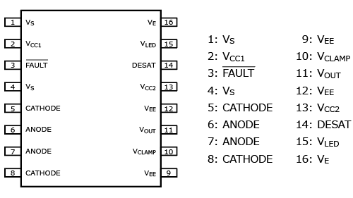
Pin Configuration

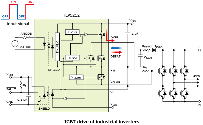
Application Circuit Example

Note :
The application circuits shown in this document are provided for reference purposes only. Thorough evaluation is required, especially at the mass-production design stage.
Providing these application circuit examples does not grant any license for industrial property rights.
* Information in this document, including product prices and specifications, content of services and contact information, is current on the date of the announcement but is subject to change without prior notice.