
Small, surface mount LDO regulators that allow long and stable operation of IoT equipment and wearable devices: TCR3UM series
Product News 2018-08
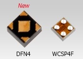
Toshiba Electronic Devices & Storage Corporation ("Toshiba") has launched 36 LDO regulator products under the "TCR3UM series", which are packed in the general purpose DFN4 package[1], for IoT equipment and wearable devices that feature low consumption current. The products are small, surface mount LDO regulators with 300 mA output (max) using state of the art CMOS process.
Electronics devices such as communication devices are increasingly equipped with coin or lithium-ion batteries. Mobile devices such as smart phones and tablets consume large current and are expected to be frequently charged. On the other hand, IoT sensors sending temperature or flow rate data used in agricultural or industrial equipment and wearable devices equipped with communication functions are required to operate long hours with less frequent battery charging or replacement, and also require stable and precise power supplies. Therefore, LDO regulators used as power supply ICs are also required to feature low consumption current allowing long time operation under low power as well as stable output voltage.
To meet such demand, Toshiba started mass production of our TCR3UG series products in September 2017. Our TCR3UG series products use the small and thin WCSP4F package[2], as well as achieve the industry’s best[3] trade-off between low consumption current characteristics and high ripple rejection ratio and high speed load transient response. In addition, TCR3UM series products using the general-purpose DFN4 package[1] have been released this time.
The new TCR3UM series products allow longer time battery drive and stable operation of sensors and CPUs that are susceptible to voltage fluctuation such as noise. They also incorporate protection functions such as overheat protection, overcurrent protection and rush current suppression. 36 products with output voltages which ranges from 0.8 V to 5.0 V have been mass-produced, allowing product selection depending on the applications.
Notes:
[1] General purpose DFN4 package: 1.0×1.0 mm (typ.), t=0.60 mm (max)
[2] Small and thin WCSP4F package: 0.645×0.645 mm (typ.), t=0.33 mm (max)
[3] By an output current 300 mA LDO regulator, as of July 10, 2018, from a survey by Toshiba.
Features
- Low consumption current (Low quiescent current): IB(ON1)=0.34 μA (typ.)
- High ripple rejection ratio, high speed road transient response: R.R.=70 dB (typ.), ⊿VOUT= -51/+36 mV (typ.)
- General-purpose DFN4 package: 1.0×1.0 mm (typ.), t=0.60 mm (max)
Applications
- IoT equipment
- Wearable devices
- Smart phones
Product Specifications
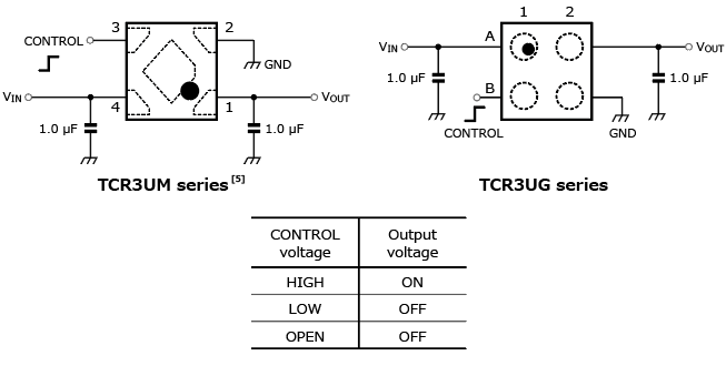
| Part number | TCR3UM series[5] | TCR3UG series | |
|---|---|---|---|
| Package | Name |  DFN4 |
 WCSP4F |
| Size typ. (mm) | 1.0×1.0, t=0.60 (max) |
0.645×0.645, t=0.33 (max) |
|
| Operating ranges | Output current IOUT max (mA) | 300 | 300 |
| Output voltage VOUT (V) | 0.8 to 5.0 | 0.8 to 5.0 | |
| Input voltage VIN (V) @IOUT=1 mA |
1.5 to 5.5 | 1.5 to 5.5 | |
| Operating temperature Topr (°C) | -40 to 85 | -40 to 85 | |
| Electrical characteristics (Unless otherwise specified, @Tj=25 °C) |
Quiescent current IB(ON1) typ. (μA) @VOUT≤1.5 V, IOUT=0 mA[4] |
0.34 | 0.34 |
| Ripple rejection ratio R.R. typ. (dB) @VRipple=200 mVp-p, IOUT=10 mA, f=1 kHz, Ta=25 °C[4] |
70 | 70 | |
| Drop-out voltage VDO typ. (mV) @VOUT=3.3 V, IOUT=300 mA[4] |
196 | 140 | |
| Load transient response ⊿VOUT typ. (mV) @VOUT=0.8 V, VIN=3.3 V, IOUT=1→50 mA/50→1 mA[4] |
-51/+36 | -60/+60 | |
Notes:
[4] Common test conditions: Unless otherwise specified, @VIN=VOUT+1 V (VOUT>1.5 V), VIN=2.5 V (VOUT≤1.5 V), IOUT=50 mA, CIN=1.0 μF, COUT=1.0 μF
[5] New products
Lineup
TCR3UM series[5]
| No. | Output voltage typ. (V) |
Auto-discharge | No. | Output voltage typ. (V) |
Auto-discharge |
|---|---|---|---|---|---|
| Yes | Yes | ||||
| 1 | 0.8 | 19 | 1.9 | ||
| 2 | 0.85 | 20 | 2.5 | ||
| 3 | 0.9 | 21 | 2.6 | ||
| 4 | 0.95 | 22 | 2.7 | ||
| 5 | 1.0 | 23 | 2.8 | ||
| 6 | 1.05 | 24 | 2.85 | ||
| 7 | 1.1 | 25 | 2.9 | ||
| 8 | 1.15 | 26 | 2.925 | ||
| 9 | 1.2 | 27 | 3.0 | ||
| 10 | 1.3 | 28 | 3.1 | ||
| 11 | 1.35 | 29 | 3.2 | ||
| 12 | 1.4 | 30 | 3.3 | ||
| 13 | 1.5 | 31 | 3.5 | ||
| 14 | 1.6 | 32 | 3.6 | ||
| 15 | 1.75 | 33 | 4.1 | ||
| 16 | 1.8 | 34 | 4.2 | ||
| 17 | 1.825 | 35 | 4.5 | ||
| 18 | 1.85 | 36 | 5.0 |
TCR3UG series
| No. | Output voltage typ. (V) |
Auto-discharge | No. | Output voltage typ. (V) |
Auto-discharge | ||
|---|---|---|---|---|---|---|---|
| Yes | No | Yes | No | ||||
| 1 | 0.8 | 17 | 2.5 | ||||
| 2 | 0.85 | 18 | 2.6 | ||||
| 3 | 0.9 | 19 | 2.7 | ||||
| 4 | 0.95 | 20 | 2.8 | ||||
| 5 | 1.0 | 21 | 2.85 | ||||
| 6 | 1.05 | 22 | 3.0 | ||||
| 7 | 1.1 | 23 | 3.1 | ||||
| 8 | 1.15 | 24 | 3.2 | ||||
| 9 | 1.2 | 25 | 3.3 | ||||
| 10 | 1.3 | 26 | 3.5 | ||||
| 11 | 1.35 | 27 | 3.6 | ||||
| 12 | 1.5 | 28 | 4.1 | ||||
| 13 | 1.75 | 29 | 4.2 | ||||
| 14 | 1.8 | 30 | 4.5 | ||||
| 15 | 1.85 | 31 | 5.0 | ||||
| 16 | 1.9 | - | - | - | - | ||
Pin Assignment and Application Circuit Example
The application circuits shown in this document are provided for reference purposes only. Thorough evaluation is required, especially at the mass-production design stage. Toshiba Electronic Devices & Storage Corporation does not grant any license to any industrial property rights by providing these examples of application circuits.
Information in this document, including product prices and specifications, content of services and contact information, is correct on the date of the announcement but is subject to change without prior notice.