
Lineup expansion of 100 V N-channel power MOSFET U-MOSIX-H series products that help improve the efficiency of power supplies: TK2R9E10PL, etc.
Product News 2018-03
Document Download (PDF:620KB)

The 12 products including “TK2R9E10PL” are new products in the 100 V N-channel power MOSFET U-MOSIX-H series suitable for power supply applications.
The new products expanding the lineup are five TO-220 package products, five TO-220SIS package products, and two DPAK package products. By using the latest generation process U-MOSIX-H with a low voltage trench structure, they feature industry’s lowest level[1] On-resistance and have improved the tradeoff between the On-resistance and output charge[2]. In addition, they have inherited the low gate switch charge characteristics from the existing generation process U-MOSVIII-H, reducing the product of On-resistance and gate switch charge[3], a performance requirement index in switching applications.
Notes:
[1] As of January 2018, from a survey by Toshiba Electronic Devices & Storage Corporation.
[2] TK2R9E10PL has improved its product of On-resistance (typ.) and output charge (typ.) by about 18 % compared with TK100E10N1 (U-MOSVIII-H).
[3] TK2R9E10PL has improved its product of On-resistance (typ.) and gate switch charge (typ.) by about 25 % compared with TK100E10N1 (U-MOSVIII-H).
Features
- Industry’s lowest level On-resistance[1]
RDS(ON)=2.9 mΩ (max) @VGS=10 V (TK2R9E10PL) - Low output charge and low gate switch charge
- Allows 4.5 V logic level drive
Applications
- Various types of power supplies
(efficient DC-DC converters, efficient AC-DC converters, switching power supplies, etc.) - Motor control equipment (motor drives, etc.)
Product Specifications
(Unless otherwise specified, @Ta=25 °C)
| Part number |
Absolute maximum ratings |
Drain-source On-resistance RDS(ON) max (mΩ) |
Total gate charge Qg typ. (nC) |
Gate switch charge QSW typ. (nC) |
Output charge Qoss typ. (nC) |
Input capacitance Ciss typ. (pF) |
Package | ||
|---|---|---|---|---|---|---|---|---|---|
| Drain- source voltage VDSS (V) |
Drain current (DC) ID @TC=25 °C (A) |
@VGS =10 V |
@VGS =4.5 V |
||||||
| 100 | 100 | 2.9 | 4.1 | 161 | 48 | 164 | 9500 | TO-220 | |
| 100 | 3.9 | 5.8 | 96 | 26 | 99 | 6320 | |||
| 70 | 6.4 | 9.7 | 58 | 17 | 58 | 3455 | |||
| 60 | 7.2 | 11 | 44 | 13 | 47 | 2800 | |||
| 42 | 10.7 | 16 | 33 | 9.3 | 32 | 2040 | |||
| 100 | 3.2 | 4.3 | 161 | 48 | 164 | 9500 | TO-220SIS | ||
| 80 | 4.1 | 5.9 | 104 | 29 | 99 | 6320 | |||
| 56 | 6.7 | 10.1 | 58 | 17 | 58 | 3455 | |||
| 50 | 7.4 | 11.2 | 44 | 13 | 47 | 2800 | |||
| 36 | 10.8 | 16 | 33 | 9.3 | 32 | 2040 | |||
| 55 | 7.7 | 11.5 | 44 | 13 | 47 | 2800 | DPAK | ||
| 40 | 10.6 | 16 | 33 | 9.3 | 32 | 2040 | |||
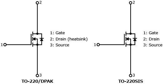
Internal Circuit
Application Circuit Example
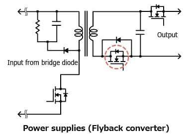
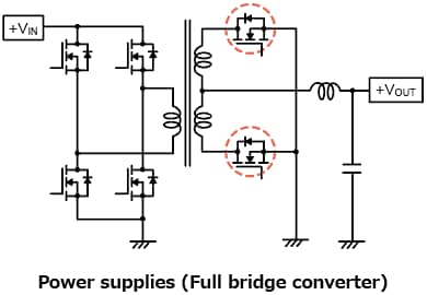
The application circuits shown in this document are provided for reference purposes only. Thorough evaluation is required, especially at the mass-production design stage. Toshiba Electronic Devices & Storage Corporation does not grant any license to any industrial property rights by providing these examples of application circuits.
Information in this document, including product prices and specifications, content of services and contact information, is correct on the date of the announcement but is subject to change without prior notice.