
Lineup Expansion of 1.5 W MOSFET Products that Use The Small TSOP6F Package and Help Reduce The Size of Equipment
Product News 2022-3
Toshiba Electronic Devices & Storage Corporation ("Toshiba") has expanded its lineup by adding two MOSFET products that use the small and high allowable power dissipation TSOP6F package. The products are suitable for applications such as motor control of consumer equipment and industrial equipment. They are the 20 V N-channel “SSM6K824R” and -30 V P-channel “SSM6J825R.”
The new products feature low On-resistance with Toshiba’s new process. In addition, the TSOP6F package has expanded the chip mounting capability with its flat leads, reducing their thermal resistance. Accordingly, the products feature a power dissipation rating of 1.5 W, helping reduce the power consumption of equipment. Furthermore, the TSOP6F package has reduced the mounting area by about 70 % compared to the Toshiba’s SOP-8 package with a similar power dissipation rating, helping reduce the size of equipment.
As a result of this addition to the lineup, we now offer six N-channel[1] and three P-channel[1] single-type MOSFET products that use the TSOP6F package, allowing users to select from a wider range of products.
Notes :
[1] As of February 2022.
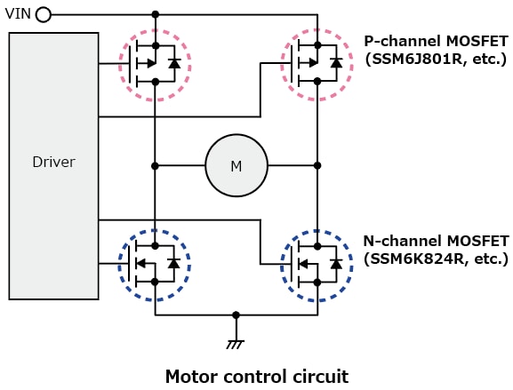
Applications
- Consumer equipment, industrial equipment (motor control circuits, power management switches, etc.)
Features
- Small TSOP6F package: 2.9 mm × 2.8 mm × 0.80 mm (typ.)
- High allowable power dissipation rating: PD=1.5 W
- Reducing power consumption with low On-resistance:
RDS(ON)=33 mΩ (max) @VGS=4.5 V (SSM6K824R)
RDS(ON)=73 mΩ (max) @VGS=-4.5 V (SSM6J825R)
Main Specifications
(@Ta=25 °C)
| Part number |
Polarity | Package | Absolute maximum ratings | Electrical characteristics | ||||||
|---|---|---|---|---|---|---|---|---|---|---|
| Name | Size typ. (mm) |
Drain- source voltage VDSS (V) |
Gate- source voltage VGSS (V) |
Drain current (DC) ID (A) |
Power dissipation PD (W) |
Drain-source On-resistance RDS(ON) max (mΩ) |
Input capacitance Ciss typ. (pF) |
Total gate charge Qg typ. (nC) |
||
| @|VGS|= 4.5 V |
||||||||||
| SSM6K824R | N-channel | TSOP6F | 2.9 × 2.8 × 0.80 | 20 | ±8 | 6 | 1.5 | 33 | 410 | 3.6 |
| SSM6K818R [2][3] |
30 | ±20 | 15 | 12.0 | 1130 | 7.5 | ||||
| SSM6K804R [2][3] |
40 | ±20 | 12 | 18 | 1110 | 7.5 | ||||
| SSM6K809R [2][3] |
60 | ±20 | 6 | 51 | 550 | 9.3 | ||||
| SSM6K810R [2][3] |
100 | ±20 | 3.5 | 92 | 430 | 3.2 | ||||
| SSM6K819R [2][3] |
100 | ±20 | 10 | 36.4 | 1110 | 8.5 | ||||
| SSM6J801R [2] |
P-channel | -20 | -8/+6 | -6.0 | 32.5 | 840 | 12.8 | |||
| SSM6J825R | -30 | -20/+10 | -4 | 73 | 492 | 6.2 | ||||
| SSM6J808R [2][3] |
-40 | -20/+10 | -7 | 48 | 1020 | 24.2 | ||||
Notes :
[2] Existing products
[3] AEC-Q101 qualified products for automobiles
Pin Assignments

Application Circuit Example
Note :
The application circuits shown in this document are provided for reference purposes only.
Thorough evaluation is required, especially at the mass-production design stage.
Providing these application circuit example does not grant any license for industrial property rights.
Information in this document, including product prices and specifications, content of services and contact information, is current on the date of the announcement but is subject to change without prior notice.