

Toshiba Develops Technology that Achieves Lower Loss and Enhanced Short-Circuit Robustness in Trench-Gate SiC MOSFETs
May 27, 2026
Toshiba Electronic Devices & Storage Corporation
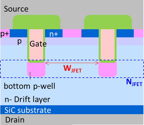
Kawasaki, Japan-Toshiba Electronic Devices & Storage Corporation ("Toshiba") has developed a technology for trench-gate silicon carbide (SiC) MOSFETs[1], a power semiconductor that reduces losses (on-resistance[2]) while enhancing short-circuit robustness[3]. The technology optimizes a bottom p-well structure[4] formed under the trench and the design of the junction field-effect transistor (JFET)[5] region within it, including its width and doping concentration.
Toshiba has confirmed that the new technology suppresses short-circuit energy generated inside the device and reduces temperature rises, achieving improved short-circuit robustness and lower loss while maintaining gate oxide reliability. These advances are expected to contribute to improved device reliability and energy efficiency in power conversion applications, including electric vehicles, renewable energy systems, and power supplies for data centers.
Power semiconductors play a critical role in the efficient control and conversion of electric power, and are essential for achieving energy savings and carbon neutrality. SiC MOSFETs are widely recognized as next-generation devices that realize more efficient power conversion than conventional silicon (Si) MOSFETs, and they are increasingly adopted in applications as diverse as electric vehicles, renewable energy systems, and data centers. Trench-gate SiC MOSFETs are characterized by their ability to achieve low on-resistance and high current density.
In trench-gate SiC MOSFETs, electric-field protection structures[6] ensure gate oxide reliability. However, the resulting JFET region influences current flow paths and thermal behavior. The relationship between the energy generated during short-circuit events (short-circuit energy) and device degradation, and its correlation with the design of the JFET region has not been fully understood, making it difficult to achieve both reduced on-resistance and improved short-circuit robustness.
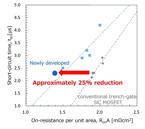
Toshiba addressed by investigating a trench-gate SiC MOSFET structure incorporating a bottom p-well under the trench. By narrowing the width of the JFET region (WJFET) and increasing its doping concentration (NJFET) (Figure 1), Toshiba confirmed suppression of short-circuit current and reduced short-circuit energy generation inside the device. The company also clarified that device degradation correlates with short-circuit energy, demonstrating that suppressing short-circuit energy is effective in improving reliability. This provides a design guideline that simultaneously achieves improved short-circuit robustness and lower on-resistance while maintaining gate oxide reliability. In prototype devices, Toshiba confirmed an approximately 25% reduction in on-resistance compared with conventional trench-gate SiC MOSFETs while maintaining short-circuit robustness (Figure 2)[7].
The technology demonstrates the effectiveness of a new design approach focusing on short-circuit energy in trench-gate SiC MOSFETs. It is expected to enable further loss reduction and contribute to improved efficiency and reliability in high-efficiency power conversion applications, including electric vehicles, renewable energy systems, and power supplies for data centers. Test samples of a 1200V trench-gate SiC MOSFET incorporating part of this technology, “TW007D120E,” have been shipping since earlier this month.
Toshiba will present details of this technology at the 38th International Symposium on Power Semiconductor Devices and ICs (ISPSD) 2026, held in Las Vegas from May 24 to 28.
This work is based on results obtained from a project, JPNP21029, subsidized by the New Energy and Industrial Technology Development Organization (NEDO).
[1] MOSFET: Metal Oxide Semiconductor Field Effect Transistor, a switching device with three electrodes: gate, drain, and source. Current between the drain and source is switched on and off by applying a gate voltage. In trench-gate MOSFETs, the gate electrode is formed within a trench structure, enabling high integration density and low on-resistance.
[2] On-resistance is the resistance value between the drain and source of a MOSFET during operation (ON).
[3] Short-circuit robustness (short-circuit withstand capability): A measure of the time or energy a device can withstand before failure under short-circuit conditions, where excessive current rapidly flows due to abnormal conditions such as a load short.
[4] Bottom p-well structure: A p-type region formed at the bottom of the trench that mitigates electric-field concentration and improves the reliability of the gate oxide.
[5] JFET: Junction Field-Effect Transistor, a type of transistor that controls current flow using an electric field and operates based on semiconductor junction structures.
[6] Electric-field protection structure: A structure that reduces the electric field applied to the gate oxide when the MOSFET is in the off state.
[7] Comparison with Toshiba’s conventional trench-gate SiC MOSFET announced on June 9, 2025. (Toshiba test results)
* Company names, product names, and service names may be trademarks of their respective companies.
* Information in this document, including product prices and specifications, content of services and contact information, is current on the date of the announcement but is subject to change without prior notice.