
Toshiba Develops SiC Power Module Technology for High-Frequency Inverters Used in Data Center Power Systems
June 12, 2026
Toshiba Electronic Devices & Storage Corporation
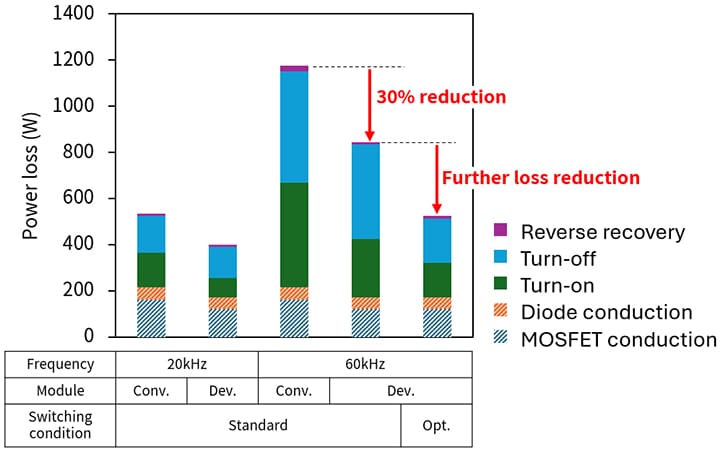
Kawasaki, Japan-Toshiba Electronic Devices & Storage Corporation ("Toshiba") has developed silicon carbide (SiC) power module technology for high-frequency inverter applications that delivers lower power loss and higher reliability. The technology combines Toshiba’s proprietary Schottky barrier diode (SBD)[1] embedded SiC MOSFET[2] with an optimized module design to realize high reliability and low loss operation during high-speed switching. Simulation results indicate that, under high-frequency inverter operation at 60kHz, total inverter power loss can be reduced by approximately 30% compared with a module using a conventional SBD-embedded SiC MOSFET structure[3].
The widespread adoption of AI and the increasing sophistication of data centers is fast raising power consumption. The power systems that support them are required to deliver higher efficiency and higher power density, which is increasing the importance of power semiconductors that operate at high frequencies. This is particularly true for power equipment such as inverters and uninterruptible power supplies (UPS) that must meet efficiency and size requirements. In these circumstances, 1200V-class SiC power modules are expected to play a central role in next-generation power systems, but this requires further improvements in chip and module design.
Toshiba has addressed reliability challenges during diode conduction associated with SiC material characteristics by developing SBD-embedded SiC MOSFETs. However, conventional device structures[3] constrain the layout of channel and SBD regions, making it difficult to balance low on-resistance[4] with diode reliability. In addition, reducing the total chip area in a power module improves switching speed but introduces trade-offs, including increased on-resistance, reduced diode reliability, and degraded thermal performance.
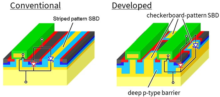
The newly developed SBD-embedded SiC MOSFET has a structure that combines a checkerboard-pattern SBD layout with a deep p-type barrier region[5] (Figure 1). Utilizing the increased design flexibility realized by the electric-field suppression[6] effect of the deep p-type barrier region, allows integrated optimization of multiple design parameters—including the channel[7], drift layer[8], JFET[9] region, and gate-drive conditions. As a result, the device suppresses localized current concentration, improves current flow through the channel and drift layer, and enables stable current operation in both on-state operation and diode operation. This improves the trade-off between on-resistance and diode reliability. The achievement of a specific on-resistance of 1.8mΩ·cm² at 25°C and 2.7mΩ·cm² at 150°C, represents an approximately 50% reduction against the typical device structure[3], and increases SBD current conduction capability[10] per unit area by approximately 40%.
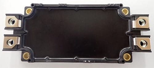
The developed device was applied to a 1200V-class SiC power module (Figure 2). The total chip area in the module was reduced by approximately 36% against the conventional structure[3]. At the same time, improved chip performance, achieved through reduced on-resistance and enhanced reliability, delivered lower module-level conduction loss[11] while maintaining diode reliability. Furthermore, improvements in the packaging structure and design, including the adoption of a resin-insulated substrate, allowed Toshiba to reduce thermal resistance per unit area by approximately 25%. This improves heat spreading and maintains heat dissipation performance even under the increased thermal density resulting from the reduction in total chip area.
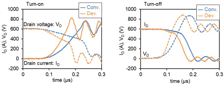
Further reduction in switching losses[12] was confirmed as a result of these improvements (Figure 3). Simulation results indicate that total inverter power loss can be reduced by approximately 30% under 60kHz high-frequency operation (Figure 4). Further reductions in switching loss are expected through optimization of switching conditions, including gate-drive speed. The results indicate that significant performance improvements can be achieved in high-frequency power conversion.
This technology is expected to serve as a key platform for achieving higher efficiency and smaller size in power conversion systems, including data center UPS, industrial equipment, and renewable energy applications. Toshiba will continue to advance development toward practical application and mass production, while further enhancing high-frequency operation and performance to improve the energy efficiency of power systems, thereby contributing to a sustainable society.
Details of this technology were presented at Power Conversion and Intelligent Motion (PCIM) Europe 2026, held in Nuremberg, Germany, from June 9 to 11, 2026.
[1] SBD (Schottky Barrier Diode): A rectifying device that allows current to flow in one direction, formed by a junction between a metal and an n-type semiconductor.
[2] MOSFET (Metal-Oxide-Semiconductor Field-Effect Transistor): A switching device with three terminals (gate, source, and drain) that controls current flow between the drain and source by applying a voltage to the gate.
[3] Conventional structure: Refers to Toshiba’s previously developed third-generation
SBD-embedded SiC MOSFET.
[4] On-resistance: The resistance between the drain and source when the MOSFET is in the on-state.
[5] Barrier region: A region formed inside the device to control high electric fields under high-voltage operation, affecting current flow and device characteristics.
[6] Electric-field suppression: The effect of reducing locally concentrated high electric fields within the device, contributing to improved current distribution and reliability.
[7] Channel: A region inside the MOSFET through which current flows during operation.
[8] Drift layer: A layer that sustains high voltage and contributes to the breakdown voltage of the device.
[9] JFET region: A region inside the MOSFET that forms part of the current conduction path and affects current flow and on-resistance.
[10] SBD current conduction capability: The ability of the embedded SBD to conduct current; higher capability enables stable current flow during diode operation.
[11] Conduction loss: Power loss that occurs when current flows through the device in the on-state, mainly determined by on-resistance.
[12] Switching loss: Power loss that occurs during switching transitions when voltage and current overlap in time.
* Company names, product names, and service names may be trademarks of their respective companies.
* Information in this document, including product prices and specifications, content of services and contact information, is current on the date of the announcement but is subject to change without prior notice.