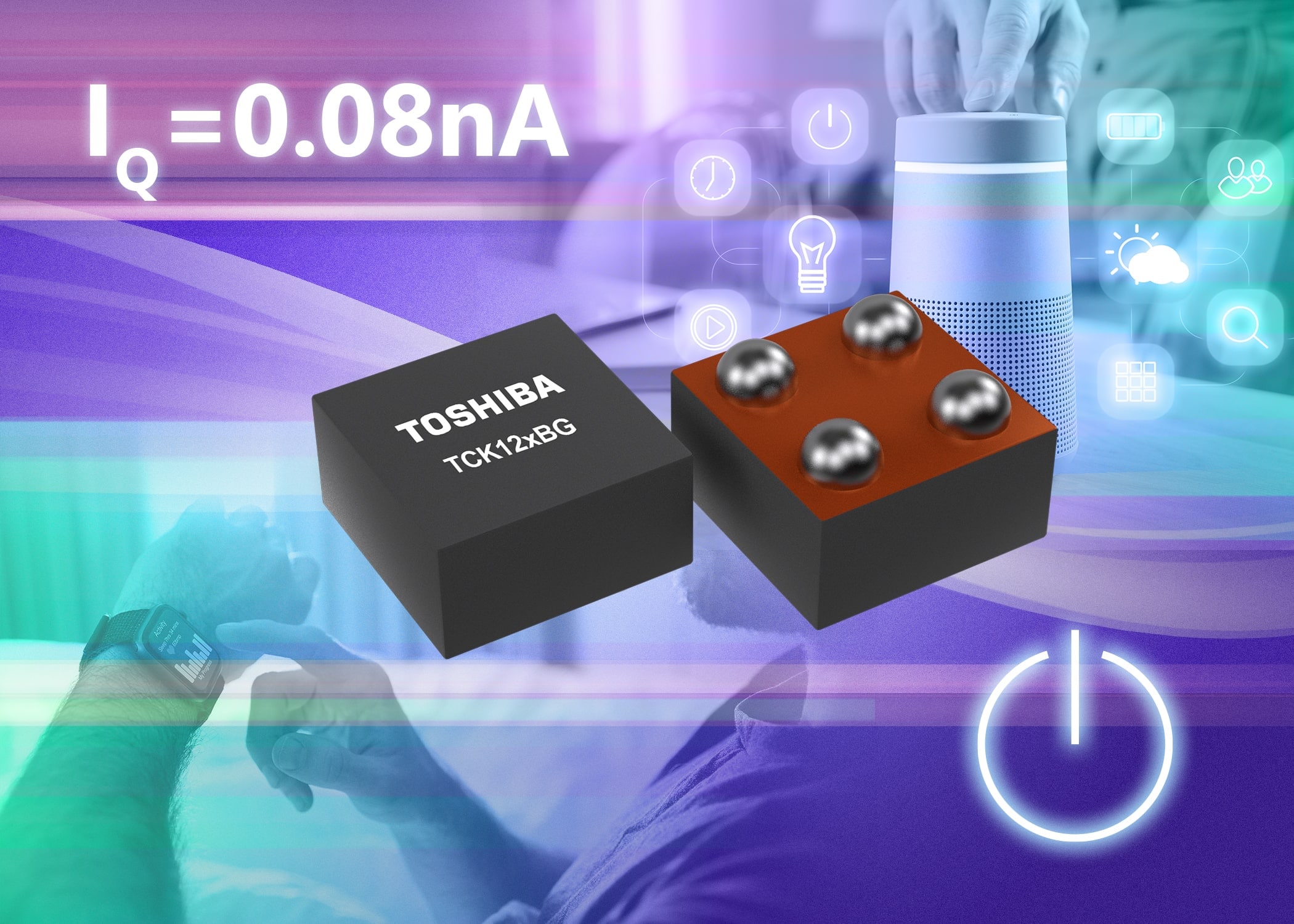
Toshiba announces load switches with ultra-low quiescent current consumption of 0.08nA
27th January 2022

Toshiba Electronics Europe GmbH (“Toshiba”) has launched three load switch products that deliver a remarkable decrease in quiescent current. The new devices are primarily intended for use in wearable and IoT applications where they will control the power supply for peripherals such as sensors. They are also useful when upgrading existing designs that are built around discrete semiconductors.
Devices in the new TCK12xBG series feature a new driver circuit that has been developed by Toshiba, thereby enabling a typical ON-state quiescent current (IQ) of just 0.08nA. It represents a reduction in the region of 99.9% from Toshiba’s current product TCK107AG. This contributes significantly to extending the operating life of wearables and IoT devices that are powered by small batteries.
There are three devices within the series. The TCK127BG offers automatic discharge that turns on at active high, the TCK126BG turns on without automatic discharge, and the TCK128BG at an active low. The devices operate from a supply (VIN) and control (VCT) voltage in the range -0.3V to 6.0V. The output current (IOUT) is rated at 1.0A continuously and 2.0A for pulsed operation.
All of the new TCK12xBG devices are housed in a recently developed WCSP4G package that occupies just 0.645mm x 0.645mm of board area with a height of 0.465mm, significantly saving space in compact wearable and IoT designs. An innovative backside coating reduces the possibility of damage to the devices during the mounting process.
Toshiba will continue to develop and enhance products utilizing their low quiescent current technology to contribute to reduced consumption of equipment and smaller devices.
Shipment of all three TCK12xBG devices starts today.