
Toshiba starts test-sample shipments of 1200V trench-gate SiC MOSFET for next-generation AI data centers
21st May 2026

Toshiba Electronics Europe GmbH (“Toshiba”) has today started test-sample shipments of the TW007D120E, 1200V trench-gate SiC MOSFET primarily intended for power supply systems in AI data centers. Housed in a QDPAK top-side cooled package, the surface mount device delivers high current capability, improved heat dissipation, and higher power density in the power stage, which is essential for power conversion in AI data centers. The product is also suitable for renewable energy-related equipment, including photovoltaic inverters, uninterruptible power supplies (UPS), EV charging stations, and energy storage systems.
With the rapid expansion of generative AI, increasing power consumption has become a pressing issue for data centers. In particular, the widespread adoption of high-power AI servers and the growing deployment of 800V HVDC (high voltage direct current) architectures are driving demand for power supply systems with higher power conversion efficiency and power density. The TW007D120E addresses these requirements, combining low conduction loss, low switching loss, and enhanced thermal performance to support more efficient and compact power system designs.
The new MOSFET features Toshiba’s proprietary trench-gate structure, which achieves a remarkably low On-resistance per unit area (RDS(on)A). The typical RDS(on) of the device is 7.0mΩ with 33nC gate-drain charge (Qgd) and 172A DC drain current (ID). Compared with Toshiba’s 3rd-generation 1200V SiC MOSFET (TW015Z120C), the TW007D120E reduces RDS(on)A by approximately 58% and improves the figure of merit (RDS(on) × Qgd), which represents the trade-off between conduction loss and switching loss, by approximately 52%. The device also supports low gate drive voltage (Vgs-on) operation of 15V to 18V. These features enable highly efficient operation and reduced heat generation in data center power supply systems, contributing to improved overall system performance.
Toshiba plans to prepare for mass production of the TW007D120E during fiscal year 2026 and will continue to expand its lineup, including development for automotive applications. Through its trench-gate SiC MOSFET technology, Toshiba aims to contribute to improved power efficiency and reduced CO₂ emissions across data centers and industrial equipment, thereby supporting the realisation of a decarbonised society.
News Links
Main Specifications
(Unless otherwise specified, Tvj=25°C)
| Part number | TW007D120E | |||
|---|---|---|---|---|
| Package | Name | QDPAK | ||
| Absolute maximum ratings |
Drain-source voltage VDSS (V) | 1200 | ||
| Drain current (DC) ID (A) | Tc=25°C | 172 | ||
| Electrical character- istics |
Drain-source On-resistance RDS(on) (mΩ) |
VGS=15V | Typ. | 7.0 |
| Gate threshold voltage Vth (V) | VDS=10V | 3.0 to 5.0 | ||
| Total gate charge Qg (nC) | VGS=15V | Typ. | 317 | |
| Gate-drain charge Qgd (nC) | VGS=15V | Typ. | 33 | |
| Input capacitance Ciss (pF) | VDS=800V | Typ. | 13972 | |
| Diode forward voltage VSD (V) | VGS=0V | Typ. | 3.2 | |
Note: Specifications and schedules for products under development are subject to change without notice.
Performance Comparison Charts
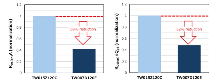
Test conditions: VGS=18V (TW015Z120C), VGS=15V (TW007D120E), Tvj=25°C. Toshiba research as of May 2026.
Follow the link below for more on Toshiba’s SiC Power Devices.
SiC Power Devices
* Company names, product names, and service names may be trademarks of their respective companies.
* Information in this document, including product prices and specifications, content of services and contact information, is current on the date of the announcement but is subject to change without prior notice.