
Toshiba Releases 650V 3rd Generation SiC MOSFETs in DFN8×8 Package
May 20, 2025
Toshiba Electronic Devices & Storage Corporation

KAWASAKI, Japan—Toshiba Electronic Devices & Storage Corporation ("Toshiba") has launched four 650V silicon carbide (SiC) MOSFETs, equipped with its latest[1] 3rd generation SiC MOSFET chips and housed in a compact DFN8×8 package, suitable for industrial equipment, such as switched-mode power supplies and power conditioners for photovoltaic generators. Volume shipments of the four devices, “TW031V65C,” “TW054V65C,” “TW092V65C,” and “TW123V65C,” start today.
The new products are the first 3rd generation SiC MOSFETs to use the small surface-mount DFN8×8 package, which reduces volume by more than 90% compared to lead-inserted packages, such as TO-247 and TO-247-4L(X) and improves equipment power density. Surface mounting also allows use of parasitic impedance[2] components smaller than those of lead-inserted packages, reducing switching losses. DFN8×8 is a 4-pin[3] package, allowing use of a Kelvin connection of its signal source terminal for the gate drive. This reduces the influence of inductance in the source wire within the package, achieving high-speed switching performance; in the case of TW054V65C, it reduces turn-on loss by approximately 55% and turn-off loss by approximately 25%[4] compared to current Toshiba products[5], helping to reduce power loss in equipment.
Toshiba will continue to expand its lineup to contribute to improved equipment efficiency and increased power capacity.
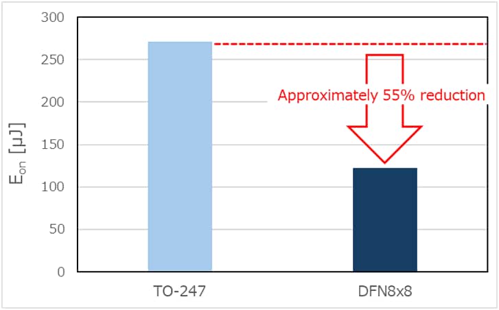
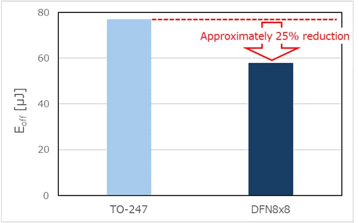
Measurement condition: VDD=400V, VGS=18V/0V, ID=20A, Ta=25°C, L=100μH, Rg (external gate resistor) =4.7Ω
The freewheeling diode uses the diode between the source and drain of each product.
(Toshiba comparison, as of May 2025)
Figure 1. Comparison of turn-on loss (Eon) and turn-off loss (Eoff) between TO-247 and DFN8×8 package
Notes:
[1] As of May 2025.
[2] Resistance, inductance, etc.
[3] A product with a signal-source pin connected close to the FET chip.
[4] As of May 2025, values measured by Toshiba. Please refer to Figure 1.
[5] A 650V 3rd generation SiC MOSFET with equivalent voltage and On-resistance that uses the TO-247 package without Kelvin connection.
Applications
- Switched mode power supplies in servers, data centers, communications equipment, etc.
- EV charging stations
- Photovoltaic inverters
- Uninterruptible power supplies
Features
- DFN8×8 surface-mount package. Enables equipment miniaturization of and automated assembly. Low switching loss.
- Toshiba’s 3rd generation SiC MOSFETs
- Good temperature dependence of drain-source On-resistance by optimization of drift resistance and channel resistance ratio
- Low drain-source On-resistance×gate-drain charges
- Low diode forward voltage: VDSF=-1.35V(typ.) (VGS=-5V)
Main Specifications
(Unless otherwise specified, Ta=25°C)
| Part number | TW031V65C | TW054V65C | TW092V65C | TW123V65C | |||
|---|---|---|---|---|---|---|---|
| Package | Name | DFN8×8 | |||||
| Size (mm) | Typ. | 8.0×8.0×0.85 | |||||
| Absolute maximum ratings |
Drain-source voltage VDSS (V) | 650 | |||||
| Gate-source voltage VGSS (V) | -10 to 25 | ||||||
| Drain current (DC) ID (A) | Tc=25°C | 53 | 36 | 27 | 18 | ||
| Electrical character -istics |
Drain-Source On-resistance RDS(ON) (mΩ) | VGS=18V | Typ. | 31 | 54 | 92 | 123 |
| Gate threshold voltage Vth (V) | VDS=10V | 3.0 to 5.0 | |||||
| Total gate charge Qg (nC) | VGS=18V | Typ. | 65 | 41 | 28 | 21 | |
| Gate-drain charge Qgd (nC) | VGS=18V | Typ. | 10 | 6.2 | 3.9 | 2.3 | |
| Input capacitance Ciss (pF) | VDS=400V | Typ. | 2288 | 1362 | 873 | 600 | |
| Diode forward voltage VDSF (V) | VGS=-5V | Typ. | -1.35 | ||||
| Sample Check & Availability |  |
|
|
|
|||
Related links
Features of third generation SiC MOSFET (PDF: 1,318KB)
FAQ SiC MOSFET (PDF: 818KB)
Comparison of SiC MOSFET and Si IGBT (PDF: 922KB)
SiC MOSFET Absolute Maximum Ratings and Electrical Characteristics (PDF: 812KB)
Follow the link below for more on Toshiba’s SiC Power Devices.
SiC Power Devices
To check availability of the new products at online distributors, visit:
TW031V65C
TW054V65C
TW092V65C
TW123V65C
Customer Inquiries:
Power & Small Signal Device Sales & Marketing Dept.
Tel: +81-44-548-2216
* Company names, product names, and service names may be trademarks of their respective companies.
* Information in this document, including product prices and specifications, content of services and contact information, is current on the date of the announcement but is subject to change without prior notice.