
8th October 2019
Tiny device features lower input power to reduce equipment size and power consumption
Toshiba Electronics Europe (“Toshiba”) announces the availability of a new voltage driven photorelay with a tiny S-VSON4T package and reduced input power dissipation.
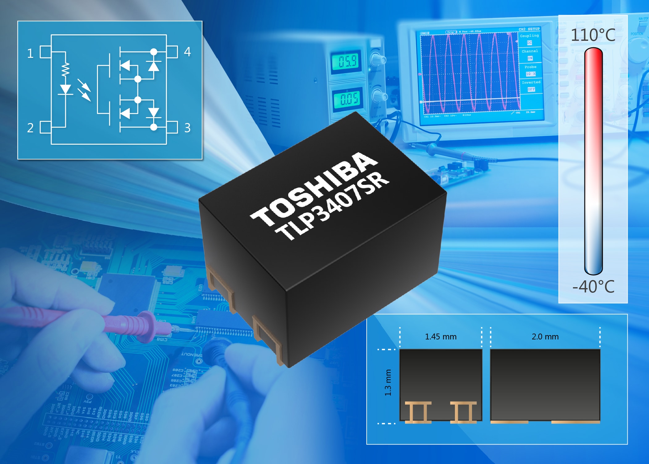
The new product, designated TLP3407SR, features a maximum LED current of just 1 mA at the input, which represents a reduction to approximately 33% of that of its predecessor, the TLP3407SRH. This allows the product to offer a maximum input power dissipation of 3.3 mW. For use with higher voltages of 5 V or more, the new device can be powered by adding an external resistor in series, allowing designers to implement a maximum trigger LED current of 0.2 mA. This expands the range of permissible input voltages, simplifying the task of circuit design.
With the reduced input power dissipation, the new voltage drive photorelay is suitable for reducing the power consumption of a wide variety of equipment including probe cards, automatic semiconductor test equipment (ATE), semiconductor testers, and other similar applications.
The TLP3407SR is housed in a tiny S-VSON4T package that features a mounting area / footprint of just 2.9 mm2 - a reduction of around 27% when compared to the existing VSONR4 package. As a result, this new product can help reduce the size of end products or increase the number of photorelays that can be mounted in a fixed space.
For more information about the new product and the wider line-up, please visit:
News Links


High Resolution Image (jpg)