4-bit level shifter that helps to reduce the power consumption of automotive equipment: TC7MP3125FK
Product News 2019-03

Toshiba Electronic Devices & Storage Corporation ("Toshiba") has launched “TC7MP3125FK,” a 4-bit level shifter suitable for a unit that integrates interfaces with different power supply voltages, such as IVI (In-vehicle infotainment) equipment.
The new product, TC7MP3125FK, is a high-speed CMOS 4-bit bidirectional bus transceiver that allows two units with power supply voltages from 1.1 V to 3.6 V to interface with each other. With its 4-bit configuration, it can support interface standards such as UART, SPI, and so on. By optimizing its circuit configuration, it features an industry-leading[1] quiescent supply current of 2.0 μA (max)[2], which can help to reduce the power consumption of equipment.
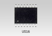
This product uses the small surface mount type (lead type) US16 package, helping to reduce mounting area. Furthermore, the flow-through layout of its I/O terminals allows easy design of PCB layouts. In addition, this product supports automated optical inspection (AOI).
We are also planning to develop a product housing same chip in the industry standard TSSOP surface mount type (lead type) package[3] to meet various package requirements.
In the automobile industry, advanced driver-assistance systems (ADAS) are increasingly being implemented due to the growing demand for safety functions. As ADAS functions become more and more sophisticated for automated driving, the number of sensors equipped in a vehicle such as cameras, radars and LiDAR (Light detection and ranging) sensors is increasing. This raises the power consumption of automotive systems, leading to demand for lower power consumption. To reduce power consumption, SoCs (System on chips) used in IVI device designs are increasingly based on low voltage SoCs developed for mobile devices. In connecting such low voltage SoCs with multiple ADASs, power supply voltage differences between units may become an issue. When two units with different power supply voltages are connected as they are, it might cause malfunctioning or IC breakdowns, so level shifters are required to translate power supply voltages.
Notes:
[1] Comparison with the product of the same maximum rating, according to a survey by Toshiba (as of January 2019).
[2] @VCCA=1.1 to 2.7 V, VCCB=1.65 to 3.6V, VINA=VCCA or GND, VINB=VCCB or GND, Ta=-40 to 85 °C
[3] Mass production planned for 2019 2Q (CY)
Features
- Allows two units from 1.1 V to 3.6 V to be bidirectionally interfaced with each other.
- Low quiescent supply current: ICCA, ICCB=2.0 μA (max)[2]
- Its package is the small US16 (4.0 x 4.0 x 0.8 mm) supporting AOI and the I/O terminals’ layout is a flow-through type.
Applications
- Automotive equipment (IVI, etc.)
- Consumer equipment
Product Specifications
| Part number | |||
|---|---|---|---|
| Package | US16 | ||
| Operating ranges (@Topr=-40 to 85 °C) |
Supply voltage |
VCCA (V) | 1.1 to 2.7 |
| VCCB (V) | 1.65 to 3.6 | ||
| Electrical characteristics (Unless otherwise specified, @Ta=-40 to 85 °C) |
Input leakage current IIN max (μA) @VIN (DIR, OE)=0 to 3.6 V |
±1.0 | |
| Power-off leakage current IOFF max (μA) @VIN, VOUT=0 to 3.6 V |
2.0 | ||
| Quiescent supply current |
ICCA max (μA) @VINA=VCCA or GND, VINB=VCCB or GND |
2.0 | |
| ICCB max (μA) @VINA=VCCA or GND, VINB=VCCB or GND |
2.0 | ||
| Propagation delay time (Bn→An) tPLH/tPHL max (ns) @VCCA=1.8±0.15 V, VCCB=3.3±0.3 V |
8.9 | ||
| Propagation delay time (An→Bn) tPLH/tPHL max (ns) @VCCA=1.8±0.15 V, VCCB=3.3±0.3 V |
7.8 | ||
| Power dissipation capacitance @Ta=25 °C, VCCA=2.5 V, VCCB=3.3 V |
CPDA typ. (pF) @OE=L, A→B (DIR=H) |
3 | |
| CPDA typ. (pF) @OE=H, A→B (DIR=H) |
0 | ||
| CPDB typ. (pF) @OE=L, A→B (DIR=H) |
16 | ||
| CPDB typ. (pF) @OE=H, A→B (DIR=H) |
0 | ||
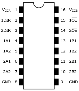
Pin Assignment

Application Circuit Examples

The application circuits shown in this document are provided for reference purposes only. Thorough evaluation is required, especially at the mass-production design stage.
Providing these application circuit examples does not grant any license for industrial property rights.
Information in this document, including product prices and specifications, content of services and contact information, is correct on the date of the announcement but is subject to change without prior notice.