Single-supply 4-bit level shifters for automotive use that allows easier design of voltage level translation circuits : 74LV4T125FK, 74LV4T125FT, 74LV4T126FK, 74LV4T126FT
Product News 2020-03

Toshiba Electronic Devices & Storage Corporation (“Toshiba”) has launched single-supply 4-bit level shifters—”74LV4T125FK,” “74LV4T125FT,” “74LV4T126FK,” and “74LV4T126FT”—that are suitable for systems that have integrated interfaces with different power supply voltages such as In-vehicle Infotainment (IVI) equipment.
The new products are single-supply types that do not require consideration to power-on sequence or voltage setting between two power supplies which have been restrictions for dual-supply types, allowing voltage level translation circuits to be designed more easily. In addition, with their low-threshold input circuit, input tolerant function and power down protection function, they can translate a wide range of voltage levels[1].
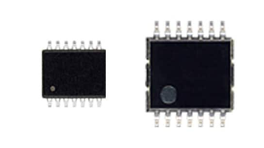
Two types of package are available : TSSOP14, a highly versatile surface-mount type, and US14, a small surface-mount type that can reduce the footprint. Both packages support appearance inspection using Automated Optical Inspection (AOI), helping improve production efficiency.
Automotive IVI systems are rapidly enhancing their multi-functional capability such as adding various functions[2] and working together with various camera functions. Along with this move is the start of platform integration similar to that in the mobile device industry, and Systems on Chip (SoCs) based on those used for mobile devices are increasingly being used. Since the basic design of SoCs for mobile devices assumes these SoCs are used in battery-driven devices for which lower power consumption is strongly required, the various voltage levels used by the SoCs tend to be low, which increases cases where voltage level differences between the SoCs and peripheral ICs/systems are causing issues[3]. To resolve such issues[3], Toshiba’s dual-supply level shifter products with two independent power supplies for the input and output sides are often used. However, to use such dual-supply level shifters, users have to consider the restrictions such as power-on sequence and voltage setting between the two power supplies. The new single-supply level shifters have eliminated such restrictions, allowing them to be used easily.
Notes :
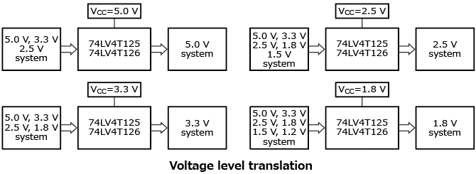
[1] Level-up voltage translation :
1.2 V to 1.8 V→1.8 V (@VCC=1.8 V)
1.5 V to 2.5 V→2.5 V (@VCC=2.5 V)
1.8 V to 3.3 V→3.3 V (@VCC=3.3 V)
2.5 V to 5.0 V→5.0 V (@VCC=5.0 V)
Level-down voltage translation :
5.0 V to 1.8 V→1.8 V (@VCC=1.8 V)
5.0 V to 2.5 V→2.5 V (@VCC=2.5 V)
5.0 V to 3.3 V→3.3 V (@VCC=3.3 V)
[2] Larger displays, higher resolutions, touch panels, high-speed radio communications, etc.
[3] Connecting systems with different voltage levels might cause malfunctioning of a system due to device malfunctioning caused by under voltage at ICs in later stages or device breakdown caused by over voltage above the ratings of ICs in later stages.
Features
- Single-supply types allowing easier design (unlike dual-supply types, restrictions such as power-on sequence and voltage setting between two power supplies do not need to be considered)
- Can translate a wide range of voltage levels[1]
- Two small surface-mount type packages supporting automatic optical inspection (US14, TSSOP14)
Applications
- Automotive equipment (IVI, ADAS[4], etc.)
- Consumer equipment
[4] ADAS (Advanced driver-assistance systems)
Product Specifications
| Part number | 74LV4T125FK | 74LV4T125FT | 74LV4T126FK | 74LV4T126FT | ||
|---|---|---|---|---|---|---|
| Control input | Active low | Active high | ||||
| Package | US14 | TSSOP14 | US14 | TSSOP14 | ||
| Operating ranges (@Topr=-40 to 125 °C) |
Supply voltage VCC (V) |
1.65 to 5.5 | ||||
| Electrical characteristics (Unless otherwise specified, @Ta=-40 to 125 °C) |
Input leakage current IIN max (µA) @VIN=0 to 5.5 V, VCC=0 to 5.5 V |
±2.0 |
||||
| 3-state output OFF-state leakage current IOZ max (µA) @VIN=VIH or VIL, VOUT=0 to 5.5 V, VCC=1.65 to 5.5 V |
±10.0 | |||||
| Power-OFF leakage current IOFF max (µA) @VIN=VIH or VIL, VOUT=0 to 5.5 V, VCC=0 V |
20.0 | |||||
| Quiescent supply current ICC max (µA) @VIN=VCC or GND, VCC=1.65 to 5.5 V |
40.0 | |||||
| Propagation delay time tPLH,tPHL max (ns) @VCC=5.0±0.5 V, CL=15 pF |
5.4 | |||||
| 3-state output enable time tPZL,tPZH max (ns) @VCC=5.0±0.5 V, CL=15 pF, RL=1 kΩ |
6.4 | 5.1 | ||||
| 3-state output disable time tPLZ,tPHZ max (ns) @VCC=5.0±0.5 V, CL=15 pF, RL=1 kΩ |
5.8 | 7.1 | ||||
| Power dissipation capacitance CPD typ. (pF) @Ta=25 °C, VCC=5.5 V |
14 | |||||
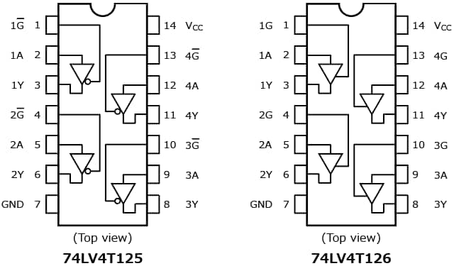
Pin Assignments

Application Circuit Examples

The application circuits shown in this document are provided for reference purposes only. Thorough evaluation is required, especially at the mass-production design stage.
Providing these application circuit examples does not grant any license for industrial property rights.
Information in this document, including product prices and specifications, content of services and contact information, is correct on the date of the announcement but is subject to change without prior notice.