
東芝研發出可降低溝槽型SiC MOSFET與Semi-Super-Junction肖特基二極體損耗的新技術
2025年6月9日
東芝電子元件及儲存裝置株式會社
日本川崎-東芝電子元件及儲存裝置株式會社(簡稱「東芝」)研發了一項創新技術,該技術可以增加溝槽型碳化矽( SiC )MOSFET [2]的UIS耐受性[3]的同時,顯著降低其因導通電阻[1]而產生的損耗。同時,東芝也研發了Semi-Super-Junction[4]肖特基二極體(SJ-SBD),有效解決了高溫下導通電阻增大的問題。這兩項技術突破可望顯著提升功率轉換器件的可靠性與效率,尤其在電動車和再生能源系統等領域。
功率半導體為所有電氣設備供電並控制電力,對於節能和碳中和的實現至關重要。隨著汽車的電氣化和工業設備的微型化,功率半導體的需求將與日俱增。 SiC MOSFET尤其如此。作為下一代元件, SiC MOSFET憑藉超越傳統矽(Si)MOSFET的功率轉換效率,獲得廣泛的關注。其中,溝槽型SiC MOSFET以其獨特的溝槽式閘極降低了導通電阻, SiC肖特基二極體(SBD)則憑藉金屬與半導體接觸實現了高效的功率轉換,它們均廣泛應用於電動車和可再生能源系統等高效功率轉換領域。然而,這些應用場景通常伴隨著高溫工作環境,對可靠性和效率提升構成了嚴峻的考驗。
溝槽型SiC MOSFET需要避免閘極氧化層受到高電場的影響。然而,由於電場保護結構[6]的UIS耐用性與接地電阻[5]之間的關係尚不明確,因此要同時實現高閘極氧化層可靠性與低導通電阻極具挑戰。
此外,儘管SiC SBD能承受比傳統Si SBD更高的工作溫度,但需要面對高溫下電阻增加進而造成導通電阻變大的問題。
東芝研發了兩項關鍵技術來解決這些問題。
1.提高溝槽型SiC MOSFET的UIS耐用性的技術
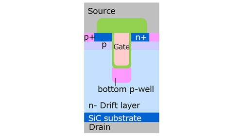
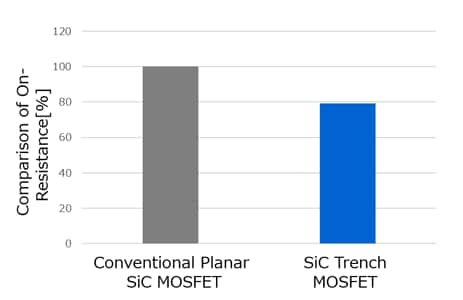
東芝研究發現,透過在溝槽型SiC MOSFET的溝槽中建構保護層(圖1),並適當降低底部p-well的接地電阻,可提高UIS耐受性。確認了以往UIS耐受性與電場保護結構接地電阻的關係的不確定性。與傳統的平面型SiC MOSFET相比,東芝製作的溝槽型SiC MOSFET原型將導通電阻降低了約20%(圖2)。
2.SiC SJ-SBD特性的改進
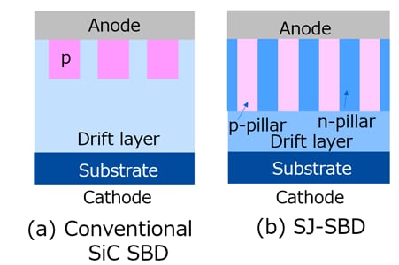
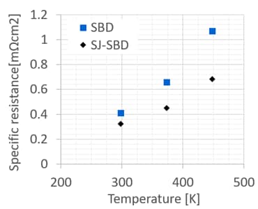
此外,東芝也研發了SiC SJ-SBD,透過在漂移層中置入柱狀結構[7]來抑制高溫下電阻的增加(圖3(b))。透過比較傳統的SiC SBD(圖3(a))和SiC SJ-SBD在不同溫度下的導通電阻變化[8] ,東芝證實了SiC SJ-SBD在高溫下具有較低的導通電阻(圖4)。這是由於Super Junction(SJ)結構實現了平坦的電場分佈並降低了導通電阻。與傳統的SiC SBD相比,東芝研發的650V SiC SJ-SBD在175 ℃ (448.15K)高溫下將導通電阻降低了約35%。
這兩項技術進一步降低了溝槽型SiC MOSFET和SiC SBD的損耗,提高了未來用於高效能功率轉換應用的裝置的可靠性和效率,尤其是在電動車和再生能源系統等領域。東芝將致力於進一步優化這些技術並加速其產業化。
在6月1日至5日於日本熊本舉行的第37屆國際功率半導體裝置與IC研討會(ISPSD 2025 ISPSD)上,東芝介紹了這些新技術的詳細資訊。此項成就是基於新能源產業技術綜合開發機構( NEDO)的專案補助而取得。
[1]導通電阻是MOSFET工作時(導通)汲極與源極之間的電阻值。
[2]MOSFET :金屬氧化物半導體場效電晶體,這是一種具有三個電極的開關元件:閘極、汲極和源極。透過向閘極施加電壓,它在汲極與源極之間切換導通和關斷電流。
[3]UIS (非箝位電感性開關)耐用性:功率元件承受開關過程中由電感性負載引起的能量突波的能力。 UIS耐用受性越高,在惡劣工作條件下的耐久性和可靠性越高。
[4]Super Junction(SJ):一種在漂移層中交替形成p型基極和n型基極的結構。
[5]接地電阻:從底部p-well結構延伸至源極金屬的總電阻。
[6]電場保護結構:溝槽型MOSFET中的一種結構特徵,減輕元件處於關閉狀態(即不導電)時對閘極氧化層的影響,有助於提高高壓條件下閘極氧化層的可靠性。
[7]柱狀結構:在漂移層內形成的摻雜半導體材料的區域。在SJ-SBD中,p型和n型基極交替排列以建構Super Junction結構。
[8]SBD的導通電阻:根據電流-電壓(IV)曲線的斜率計算得出,並減去SiC基板的電阻值。
*本文提及的公司名稱,產品名稱和服務名稱可能是其各自公司的商標。
*本文檔中的產品價格和規格、服務內容和聯絡方式等信息,在公告之日仍為最新信息,如有變更,恕不另行通知。