Small MOSFETs Bring Lower Power Consumption and Longer Operating Times to Battery-Driven Devices
Product News 2024-10

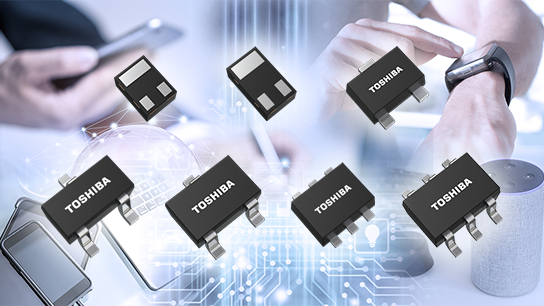
Toshiba Electronic Devices & Storage Corporation ("Toshiba") has launched small MOSFETs featuring low gate leakage current and low drain cut-off current for portable equipment and IoT devices such as wearable devices and tablet devices.
The new products have significantly reduced the drain cut-off current to 60nA (max)[1] compared with 1μA (max)[2] of Toshiba existing MOSFET products and guarantee a gate leakage current of 50nA (max) under gate-voltage conditions when the MOSFETs are in the on state (at VGS=5V)[2]. These characteristics are suitable for applications that require to minimize total energy increased by high-density design of semiconductor devices and for battery-powered portable devices. They significantly help energy saving and battery longevity of the equipment.
The new products are 29 types of 6 series: 4 series of 30V and 20V N-channel MOSFETs and 2 series of -20V P-channel MOSFETs. A variety of small surface mount packages are available to meet the diverse needs of our customers.
Notes:
[1] In SSM3K79 series
[2] In SSM3K15A series
Applications
- Smartphones
- Wearables (Hearable devices)
- IoT devices
- Laptop PCs
- Tablets, etc.
Features
(SSM3K79 Series)
- Low drain cut-off current:IDSS = 60nA (max) (VDS=30V)
- Low gate leakage current:IGSS = 50nA (max) (VGS=±5V)
Main Specifications
(Unless otherwise specified, Ta= 25 °C)
Part number |
Polarity | Package | Absolute maximum ratings |
Electric characteristics |
||||||
|---|---|---|---|---|---|---|---|---|---|---|
| Name | Size |
Drain- |
Gate- |
Drain |
Drain |
Gate |
Drain- |
|||
VDS= |
VGS= |
❘VGS❘= |
❘VGS❘= |
|||||||
| Typ. | Max | Max | Max | Max | ||||||
| SSM3K79CTC | N-channel |
CST3C | 0.8 × 0.6 | 30 |
±20 |
0.1 |
60 | ±50 | 3.6 |
- |
| SSM3K79CT | CST3 | 1.0 × 0.6 | ||||||||
| SSM3K79MFV | VESM | 1.2 × 1.2 | ||||||||
| SSM3K79FS | SSM | 1.6 × 1.6 | ||||||||
| SSM3K79FU | USM | 2.1 × 2.0 | ||||||||
| SSM6N79FE | ES6 | 1.6 × 1.6 | ||||||||
| SSM6N79FU | US6 | 2.1 × 2.0 | ||||||||
| SSM3K78CTC | N-channel |
CST3C | 0.8 × 0.6 | 20 |
±10 |
0.25 |
80 | ±80 | - |
1.1 |
| SSM3K78MFV | VESM | 1.2 × 1.2 | ||||||||
| SSM3K78FS | SSM | 1.6 × 1.6 | ||||||||
| SSM6N78FE | ES6 | 1.6 × 1.6 | ||||||||
| SSM6N78FU | US6 | 2.1 × 2.0 | ||||||||
| SSM3K77CT | N-channel |
CST3 | 1.0 × 0.6 | 20 |
±10 |
0.2 |
80 | ±80 | - |
2.2 |
| SSM3K77MFV | VESM | 1.2 × 1.2 | ||||||||
| SSM3K77FS | SSM | 1.6 × 1.6 | ||||||||
| SSM6N77FE | ES6 | 1.6 × 1.6 | ||||||||
| SSM6N77FU | US6 | 2.1 × 2.0 | ||||||||
| SSM3K76CT | N-channel |
CST3 | 1.0 × 0.6 | 20 |
±8 |
0.8 |
200 | ±200 | - |
0.235 |
| SSM3K76MFV | VESM | 1.2 × 1.2 | ||||||||
| SSM3K76FS | SSM | 1.6 × 1.6 | ||||||||
| SSM6N76FE | ES6 | 1.6 × 1.6 | ||||||||
| SSM3J78CTC | P-channel |
CST3C | 0.8 × 0.6 | -20 |
±10 |
-0.25 |
80 | ±80 | - |
1.4 |
| SSM3J78MFV | VESM | 1.2 × 1.2 | ||||||||
| SSM3J78FS | SSM | 1.6 × 1.6 | ||||||||
| SSM6P78FE | ES6 | 1.6 × 1.6 | ||||||||
| SSM6P78FU | US6 | 2.1 × 2.0 | ||||||||
| SSM3J76CT | P-channel |
CST3 | 1.0 × 0.6 | -20 |
±8 |
-0.8 |
80 | ±80 | - |
0.39 |
| SSM3J76MFV | VESM | 1.2 × 1.2 | ||||||||
| SSM6P76FE | ES6 | 1.6 × 1.6 | ||||||||
Pin Assignments


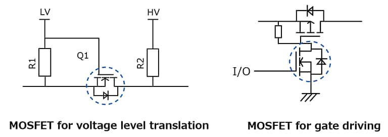
Application Circuit Examples

Note:
The application circuits shown in this document are provided for reference purposes only.
Thorough evaluation is required, especially at the mass-production design stage.
Providing these application circuit examples does not grant any license for industrial property rights.
* Company names, product names, and service names may be trademarks of their respective companies.
* Information in this document, including product prices and specifications, content of services and contact information, is current on the date of the announcement but is subject to change without prior notice.