
Toshiba小型MOSFET可降低電池驅動元件的功耗並延長其工作時間
2024年10月產品新聞

東芝電子元件及儲存裝置株式會社(簡稱「東芝」 )現針對可攜式裝置和物聯網裝置(如穿戴式裝置和平板電腦),推出了低閘極洩漏電流和低漏極截止電流的小型MOSFET 。
東芝現有MOSFET產品的汲極截止電流為1 μA (最大值) [1] ,而新型MOSFET產品將汲極截止電流顯著降低至60 nA (最大值) [2] 。因此,當MOSFET處於導通狀態( VGS = 5 V )時[1] ,新型MOSFET產品可保證在閘極電壓條件下的閘極洩漏電流為50 nA (最大值)。由於這些特性,新型MOSFET產品不僅適用於需要透過高密度半導體裝置設計來減少總能耗的應用,也適用於由電池供電的便攜式設備。新產品明顯有助於設備節能和延長電池的使用壽命。
新產品細分為6個系列、 29個型號: 30 V和20 V規格的N通道MOSFET有4個系列, -20 V規格的P通道MOSFET有2個系列。東芝可提供各種小型貼片封裝,以滿足顧客的不同需求。
註:
[ 1]SSM 3K15A系列
[2]SSM3K79系列
應用
- 智慧型手機
- 穿戴式裝置(輔聽耳機)
- 物聯網設備
- 筆記型電腦
- 平板電腦等
特點
(SSM3K79 系列)
- 低漏極截止電流:I DSS =60 nA (最大值)(V DS =30 V )
- 低閘極洩漏電流:I GSS =50 nA (最大)(V GS =±5 V )
主要規格
(在T a = 25 °C條件下,除非另有規定)
裝置型號 |
極性 | 封裝 | 絕對最大額定值 |
電氣特性 |
||||||
|---|---|---|---|---|---|---|---|---|---|---|
| 名稱 | 尺寸 |
汲極- |
閘極- |
漏極電流 |
漏極截止電流 |
閘極洩漏電流 |
漏源導通電阻 |
|||
VDS= |
VGS= |
❘VGS❘= |
❘VGS❘= |
|||||||
| 典型值 | 最大值 | 最大值 | 最大值 | 最大值 | ||||||
| SSM3K79CTC | N溝道 |
CST3C | 0.8 × 0.6 | 30 |
±20 |
0.1 |
60 | ±50 | 3.6 |
- |
| SSM3K79CT | CST3 | 1.0 × 0.6 | ||||||||
| SSM3K79MFV | VESM | 1.2 × 1.2 | ||||||||
| SSM3K79FS | SSM | 1.6 × 1.6 | ||||||||
| SSM3K79FU | USM | 2.1 × 2.0 | ||||||||
| SSM6N79FE | ES6 | 1.6 × 1.6 | ||||||||
| SSM6N79FU | US6 | 2.1 × 2.0 | ||||||||
| SSM3K78CTC | N溝道 |
CST3C | 0.8 × 0.6 | 20 |
±10 |
0.25 |
80 | ±80 | - |
1.1 |
| SSM3K78MFV | VESM | 1.2 × 1.2 | ||||||||
| SSM3K78FS | SSM | 1.6 × 1.6 | ||||||||
| SSM6N78FE | ES6 | 1.6 × 1.6 | ||||||||
| SSM6N78FU | US6 | 2.1 × 2.0 | ||||||||
| SSM3K77CT | N溝道 |
CST3 | 1.0 × 0.6 | 20 |
±10 |
0.2 |
80 | ±80 | - |
2.2 |
| SSM3K77MFV | VESM | 1.2 × 1.2 | ||||||||
| SSM3K77FS | SSM | 1.6 × 1.6 | ||||||||
| SSM6N77FE | ES6 | 1.6 × 1.6 | ||||||||
| SSM6N77FU | US6 | 2.1 × 2.0 | ||||||||
| SSM3K76CT | N溝道 |
CST3 | 1.0 × 0.6 | 20 |
±8 |
0.8 |
200 | ±200 | - |
0.235 |
| SSM3K76MFV | VESM | 1.2 × 1.2 | ||||||||
| SSM3K76FS | SSM | 1.6 × 1.6 | ||||||||
| SSM6N76FE | ES6 | 1.6 × 1.6 | ||||||||
| SSM3J78CTC | P溝道 |
CST3C | 0.8 × 0.6 | -20 |
±10 |
-0.25 |
80 | ±80 | - |
1.4 |
| SSM3J78MFV | VESM | 1.2 × 1.2 | ||||||||
| SSM3J78FS | SSM | 1.6 × 1.6 | ||||||||
| SSM6P78FE | ES6 | 1.6 × 1.6 | ||||||||
| SSM6P78FU | US6 | 2.1 × 2.0 | ||||||||
| SSM3J76CT | P溝道 |
CST3 | 1.0 × 0.6 | -20 |
±8 |
-0.8 |
80 | ±80 | - |
0.39 |
| SSM3J76MFV | VESM | 1.2 × 1.2 | ||||||||
| SSM6P76FE | ES6 | 1.6 × 1.6 | ||||||||
引腳分佈


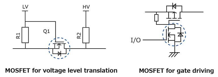
應用電路範例
註:
本文所示應用電路僅供參考。
需要進行全面評估,特別是在量產設計階段。
提供這些應用電路實例並不授予任何工業產權許可。
*本文提及的公司名稱、產品名稱和服務名稱可能是其各自公司的商標。
*本文件所載資料,包括產品價格及產品規格、服務內容及聯絡方式,僅於公告當日有效,如有更改,恕不另行通知。