
1.5 A LDO regulators in industryʼs smallest package for mobile applications: TCR15AG series
Product News 2017-12
Document Download (PDF:398KB)
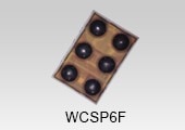
The forty-seven products in the "TCR15AG series" use the WCSP6F package, which is the smallest in the industry[1]. These products are LDO regulator ICs suitable for mobile and module applications that require smaller and lower profile products.
Despite its small package, the TCR15AG series feature high output current of 1.5 A, suiting it for power supply applications in Wi-Fi®[2] chipsets for smartphones and tablets, cameras and wireless modules.
The new series can also control power supply in applications requiring a high current, including laptop PCs, digital camcorders, storage devices and set-top boxes.
TCR15AG series deliver the industryʼs best-in-class[1] ripple rejection ratio and load transient response. They significantly reduce the ripple noise from a power management IC (PMIC) or a DC-DC converter that is often a limiting factor in the power supply for cameras and RF[3] circuits. They help to minimize output voltage fluctuations that occur in response to sharp changes in current during mode transitions in cameras and RF[3] circuits.
Low voltage dropout is secured by use of an external bias voltage pin, which helps to improve system power efficiency and contributes to longer charge life for the batteries of mobile products.
The series offers two kinds of output voltage--adjustable output between 0.60 V and 3.6 V via external resistors, and fixed output voltages from 0.65 V to 3.6 V--enabling support for a wide range of power supply applications.
Extensive protection features of the TCR15AG series include overcurrent protection and thermal shutdown, positioning it as a high-efficiency LDO solution for applications requiring highly regulated voltage in the high-current region and low power consumption.
Notes:
[1] As of November 2017 for LDO regulator ICs with an output current of 1.5 A. Toshiba Electronic Devices & Storage Corporation survey.
[2] Wi-Fi is a registered trademark of Wi-Fi Alliance.
[3] RF (Radio Frequency)
Features
- High output current of 1.5 A in the industryʼs smallest[1] WCSP6F package
- The industry's highest[1] ripple rejection ratio and fastest load transient response; highly suited to camera and RF[3] applications
- Low dropout voltage, a requirement for high-efficiency power supply applications
Applications
- Smart phones
- Tablets
Product Specifications
| Part number |
Package | Operating ranges | Electrical characteristics (@Tj=25°C) | ||||||||
|---|---|---|---|---|---|---|---|---|---|---|---|
| Name | Size typ. (mm) |
Output current IOUT (A) |
Bias voltage VBIAS min/max @VOUT≤ 1.1 V, IOUT= 1 mA (V) |
Bias voltage VBIAS min/max @VOUT> 1.1 V, IOUT= 1 mA (V) |
Output voltage VOUT typ. (V) |
Input voltage VIN min/max @IOUT= 1 mA (V) |
Quiescent current IB typ. @IOUT= 0 mA[4] (μA) |
Ripple rejection ratio R.R.(VIN) typ.[5] (dB) |
Dropout voltage VDO typ. @VBIAS= 3.3 V, IOUT= 1.5 A[6] (mV) |
Load transient response ⊿VOUT typ. @IOUT= 0.01⇔1.5 A (mV) |
|
| TCR15AG series |
WCSP6F | 1.2×0.8, t=0.33 (max) |
0 to 1.5 | 2.5/5.5 | VOUT+1.4 /5.5 |
0.65 to 3.6[7] |
VOUT+VDO /VBIAS |
25 | 95 | 120 | -100, +115 |
Notes:
[4] Not including a control pull down current (ICT) and a current flowing through an external resistor for a adjustable output voltage LDO regulator.
[5] @VBIAS=3.3 V, VIN=VOUT+1 V, IOUT=10 mA, VOUT=0.9 V, f=1 kHz, VIN Ripple=200 mVp-p, Ta=25°C, COUT=4.7 μF
[6] Measured at 0.9 V output with the TCR15AGADJ adjustable output voltage LDO regulator. VDO=VIN1*1 –(VOUT1*2 –100 mV)
*1: VIN1 is an input voltage when the output voltage drops from VOUT1 by 100 mV.
*2: VOUT1 is an output voltage when VIN=VOUT+0.5 V.
[7] 0.60 V to 3.6 V for TCR15AGADJ (adjustable output voltage type).
Lineup
| No. | Part number | Output voltage typ. (V) |
No. | Part number | Output voltage typ. (V) |
No. | Part number | Output voltage typ. (V) |
No. | Part number | Output voltage typ. (V) |
|---|---|---|---|---|---|---|---|---|---|---|---|
| 1 | 0.65 | 13 | 1.25 | 25 | 2.1 | 37 | 3.0 | ||||
| 2 | 0.7 | 14 | 1.3 | 26 | 2.2 | 38 | 3.05 | ||||
| 3 | 0.75 | 15 | 1.35 | 27 | 2.3 | 39 | 3.1 | ||||
| 4 | 0.8 | 16 | 1.4 | 28 | 2.4 | 40 | 3.2 | ||||
| 5 | 0.85 | 17 | 1.5 | 29 | 2.5 | 41 | 3.25 | ||||
| 6 | 0.9 | 18 | 1.6 | 30 | 2.6 | 42 | 3.3 | ||||
| 7 | 0.95 | 19 | 1.7 | 31 | 2.7 | 43 | 3.35 | ||||
| 8 | 1.0 | 20 | 1.75 | 32 | 2.75 | 44 | 3.4 | ||||
| 9 | 1.05 | 21 | 1.8 | 33 | 2.8 | 45 | 3.5 | ||||
| 10 | 1.1 | 22 | 1.85 | 34 | 2.85 | 46 | 3.6 | ||||
| 11 | 1.15 | 23 | 1.9 | 35 | 2.9 | 47 | Adjustable | ||||
| 12 | 1.2 | 24 | 2.0 | 36 | 2.95 | - | - | - |
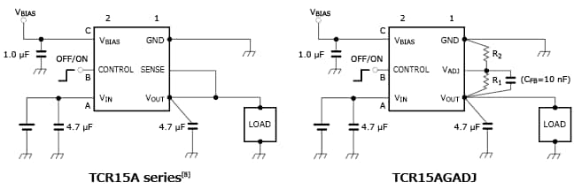
Pin Assignment and Application Circuit Example
Notes:
[8] Not for TCR15AGADJ
The application circuits shown in this document are provided for reference purposes only. Thorough evaluation is required, especially at the mass-production design stage. Toshiba Electronic Devices & Storage Corporation does not grant any license to any industrial property rights by providing these examples of application circuits.
Information in this document, including product prices and specifications, content of services and contact information, is correct on the date of the announcement but is subject to change without prior notice.