
東芝成功在降低SBD嵌入式SiC MOSFET的導通電阻的同時確保了其可靠性和短路耐受性
2024年6月3日
東芝電子元件及儲存裝置株式會社
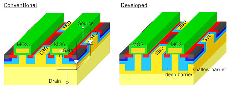
Kawasaki, Japan-Toshiba Electronic Devices & Storage Corporation (“Toshiba”) has developed a Schottky barrier diode (SBD)[1] embedded metal oxide semiconductor field effect transistor (MOSFET)[2], a significant 日本川崎-東芝電子元件及儲存裝置株式會社(簡稱「東芝」 )現已開發出一款蕭特基二極體( SBD ) [1]嵌入式金屬氧化物半導體場效電晶體( MOSFET ) [2 ] 。本產品顯著改進目前的結構的同時確保了高可靠性和短路耐受性[3] 。成功的設計升級是在裝置結構中引入了不同深度的一種勢壘結構[4] 。這種勢壘結構不僅可確保SBD反向導通操作的可靠性[5] ,同時還可抑制SBD部分的漏電流,這種漏電流會在短路期間造成元件損壞[6] 。透過利用新技術和優化結構,新型MOSFET實現了更低的導通電阻[7] ( R DS(ON) ),比現有結構降低了約26% [3] 。 .
功率半導體在電力供應和控制領域發揮核心作用,可降低各種電子設備的功耗,是實現碳中和的重要元件。隨著車輛電氣化和工業設備小型化趨勢的發展,預計功率半導體需求將繼續擴大。在此背景下, SiC MOSFET被視為下一代功率半導體。與Si MOSFET相比, SiC MOSFET的電能轉換效率更高,近年來其應用範圍迅速擴大。然而, SiC MOSFET有可靠性問題:由於反向導通操作, R DS(ON)會增加。東芝現已開發出一種內建SBD的SiC MOSFET ,可在反向導通條件下工作,並且不會增大R DS(ON) 。
減少SiC MOSFET R DS(ON)的同時,會導致短路操作期間過量電流流過MOSFET領域[6] ,進而降低短路的耐久性。然而,如果為提高反向導通操作的可靠性而增強嵌入式SBD的導通性,則會加劇短路操作期間的漏電流,這也會降低短路操作的耐久性。引入深勢壘結構可抑制短路運轉期間MOSFET的過大電流和SBD的漏電流,但它也會阻礙SBD的電流流動,引發對二極體導通可靠性下降的擔憂。 .
因此,東芝考慮將勢壘結構分為淺區和深區。深勢壘區可成功抑制短路運轉期間來自MOSFET部分的過大電流,並減少SBD電流洩漏,而淺勢壘區則可有效擴散來自SBD的電流且不受勢壘阻礙。這種方法在保持反向導通操作期間出色可靠性的同時,提高了短路的耐受性。自2023年12月以來,東芝已向部分客戶提供了採用新技術的嵌入式SBD的SiC MOSFET測試樣品用以評估,進一步提高性能。
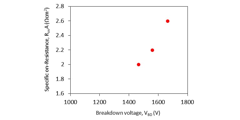
東芝利用其新設計技術並優化裝置結構,開發了原型1.2kV級SBD整合式MOSFET 。此MOSFET實現了低至2.0mΩcm 2的R DS(ON) ,與現有結構相比,導通電阻降低了約26% [3] (圖2 )。第36屆國際功率半導體裝置與IC國際會議( ISPSD 2024 )將於6月2日至6日在德國Bremen舉行,東芝將於6月3日(當地時間)出席該會議並介紹該技術的詳細資訊。
[1]SBD :蕭特基勢壘二極體,一種整流元件,可使電流沿一個方向流動,連接在金屬和n型半導體單晶內。
[2]MOSFET :金屬氧化物半導體場效電晶體,這是一種具有三個電極的開關元件:閘極、汲極和源極。透過向閘極施加電壓,它在汲極與源極之間切換導通和關斷電流。
[3]具有棋盤格圖案的SBD分佈的裝置結構,於2022年12月9日發布。
東芝開發了具有低導通電阻和高可靠性的肖特基勢壘二極體內嵌式SiC MOSFE
[4]勢壘結構:用於控制由於高壓引起的高電場的元件結構。它對元件性能有很大影響。
[5]反向導通操作:由於電路中的電流回流,電流從MOSFET的源極流向汲極的一種操作。
[6]短路操作:與正常開關操作期間的短時間導通相比,這是在控制電路故障等異常模式下會發生長時間導通的現象。要求具有在一定持續時間的短路運轉下不會失效的耐受性。
[7]導通電阻是MOSFET工作時(導通)汲極與源極之間的電阻值。
*本文提及的公司名稱、產品名稱和服務名稱可能是其各自公司的商標。
*本文件中所載資訊,包括產品價格及產品規格、服務內容及聯絡方式,僅於公告當日有效,如有更改,恕不另行通知。