TVS diodes with improved electrostatic discharge protection performance for high-speed signal lines: DF2B5M5SL, DF2B6M5SL, DF2S5M5SL, DF2S6M5SL
Product News 2018-10

Toshiba Electronic Devices & Storage Corporation ("Toshiba") has launched TVS diodes (ESD protection diodes): "DF2B5M5SL," "DF2B6M5SL," "DF2S5M5SL," and "DF2S6M5SL," which have improved their protection performance for such as high-speed signal lines for USB3.0 and HDMI®[1] from electrostatic discharge (ESD).
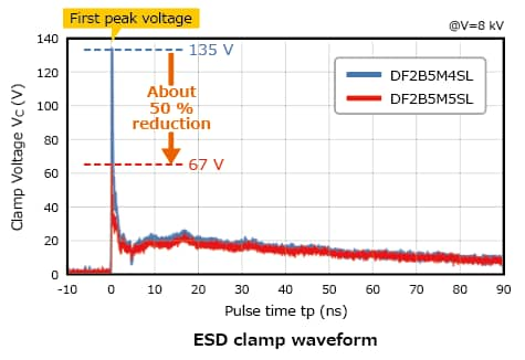
When ESD enters a device, a high surge voltage is applied to ICs and circuit components, causing them to break down or malfunction. As a measure against it, TVS diodes added in ESD penetration routes protect the ICs and circuit components by absorbing the surge voltage. The applied surge voltage is clamped at a certain voltage by the TVS diodes, but there is a range where the TVS diodes cannot adequately respond immediately after the surge, and a first peak voltage higher than the clamp voltage is applied to the ICs and circuit components. A high first peak voltage might cause malfunctions or breakdowns of ICs and circuit components.
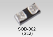
By optimizing their chip process and internal structure, the new products have reduced the first peak voltage to about 50 % compared to existing products[2] while featuring low capacitance allowing them to be used for high-speed signal lines. Protection performance is therefore improved when the new products are used for ESD protection of high-speed signal lines. In addition, as the new products use the small SOD-962 package (Toshiba’s package name: SL2), their footprints on circuit boards are small, allowing them to be used for various applications.
Notes:
[1] HDMI is a trademark or registered trademark of HDMI Licensing, LLC in the United States and/or other countries.
[2] Existing products: DF2BxM4SL series
Features (Case of DF2B5M5SL)
- Low first peak voltage: Vpeak=67 V (typ.)
- High electrostatic discharge voltage[3]: VESD= ±20 kV
- Low dynamic resistance[4]: RDYN=0.5 Ω (typ.)
Notes:
[3] @IEC61000-4-2 (Contact discharge)
[4] @TLP parameters: Z0=50 Ω, tp=100 ns, tr=300 ps, averaging window t1=30 ns to t2=60 ns
Applications
- ESD protection of a high-speed signal line
(USB connectors and HDMI®[1] connectors for smart phones, tablets and game consoles)
Product Specifications
(@Ta=25 °C)
| Part number |
Package | Polarity | Absolute maximum ratings |
Working peak reverse voltage VRWM max (V) |
First peak voltage Vpeak typ. @V=±8 kV (V) |
Dynamic resistance RDYN[4] typ. @IPP1=16 A to IPP2=30 A (Ω) |
Total capacitance Ct typ. @VR=0 V (pF) |
Clamp voltage VC[5] max @IPP=2.5 A (V) |
|
|---|---|---|---|---|---|---|---|---|---|
| Name | Size typ. (mm) |
Electrostatic discharge voltage VESD[3] (kV) |
|||||||
SOD-962 |
0.62×0.32×0.3 |
Bi- |
±20 | 3.3 | 67 | 0.5 | 0.3 | 15 | |
| ±20 | 5.0 | 70 | 0.5 | 0.3 | 15 | ||||
Single- |
±20 | 3.3 | 60 | 0.3 | 0.6 | 15 | |||
| ±20 | 5.0 | 65 | 0.3 | 0.6 | 15 | ||||
Notes:
[5] @IEC61000-4-5 8/20 μs pulse
Equivalent Circuit

Application Circuit Example

The application circuits shown in this document are provided for reference purposes only. Thorough evaluation is required, especially at the mass-production design stage. Toshiba Electronic Devices & Storage Corporation does not grant any license to any industrial property rights by providing these examples of application circuits.
Characteristic Curves (Reference)

Information in this document, including product prices and specifications, content of services and contact information, is correct on the date of the announcement but is subject to change without prior notice.