
A lineup expansion of TVS diodes for mobile devices by a product with an increased peak pulse current rating for improved surge protection performance: DF2B7BSL
Product News 2019-08
Toshiba Electronic Devices & Storage Corporation ("Toshiba") has launched the TVS diode (ESD protection diode) “DF2B7BSL” that has increased its peak pulse current rating (Ipp) to improve surge protection performance.
Ipp is a measure of protection performance against lightning surges in accordance with IEC61000-4-5. The new product features an Ipp of 7.3 A[1], which is about 83 % increase over that of the existing product DF2B7ASL. This has improved the surge protection performance, helping increase the reliability of equipment. In addition, the new product is suitable for 5 V signal line applications. For 3 V signal line applications, DF2B5BSL[2], which has been sold in advance, is available.
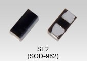
The new product uses the small SL2 package (package code: SOD-962) to allow it to be used for mobile devices such as smartphones and tablets. This can reduce the footprint.
The new product can be used for ESD protection in various applications such as audio lines, power supply lines, and general purpose input/output (GPIO).
Notes:
[1] @IEC61000-4-5
[2] A product with a different voltage from the DF2B7BSL.
Features
- High peak pulse current rating[1]: Ipp=7.3 A
- High electrostatic discharge voltage rating[3]: VESD=±30 kV
- Low clamp voltage[4]: VC=11 V (typ.) @Ipp=7.3 A
Notes:
[3] @IEC61000-4-2 (Contact)
[4] Based on IEC61000-4-5 8/20 μs pulse.
Applications
- Smart phones
- Tablets
- Game consoles, etc.
Product Specifications
(@Ta=25 °C)
| Part number |
Package | Absolute maximum ratings |
Working peak reverse voltage VRWM max (V) |
Reverse breakdown voltage VBR min/max @IBR =1 mA (V) |
Clamp voltage VC[4] typ. @Ipp =7.3 A (V) |
Dynamic resistance RDYN[5] typ. @Ipp1=8 A to Ipp2=30 A (Ω) |
Total capacitance Ct typ. @VR=0 V (pF) |
||
|---|---|---|---|---|---|---|---|---|---|
| Name (Package code) |
Size typ. (mm) |
Electrostatic discharge voltage VESD[3] (kV) |
Peak pulse current Ipp[1] (A) |
||||||
| SL2 (SOD-962) |
0.62×0.32 ×0.3 |
±30 | 7.3 | 5.5 | 5.6/7.8 | 11 | 0.2 | 12 | |
Notes:
[5] @TLP parameters: Z0=50 Ω, tp=100 ns, tr=300 ps, averaging window: t1=30 ns to t2=60 ns
Internal Circuit

Application Circuit Example

The application circuits shown in this document are provided for reference purposes only. Thorough evaluation is required, especially at the mass-production design stage. Providing these application circuit examples does not grant any license for industrial property rights.
Information in this document, including product prices and specifications, content of services and contact information, is correct on the date of the announcement but is subject to change without prior notice.