
N-channel MOSFET driver ICs in industry-leading small package for mobile and consumer applications: TCK401G, TCK402G
Product News 2017-11
Document Download (PDF:525KB)
“TCK401G” (active-high[1]) and “TCK402G” (active-low[2]) are N-channel MOSFET drivers that support an input voltage of up to 28 V, making them suitable for quick-charging and other applications requiring high current supply.
The new TCK401G and TCK402G have various built-in functions, including overvoltage protection, inrush current reducing and auto output discharge, but are still housed in the industry-leading[3] small WCSP6E package, measuring 0.8×1.2×0.55 mm (typ.).
A high-efficiency power supply circuit can be realized by using new drivers with an external N-channel MOSFET that has a maximum voltage rating and On-resistance which are suitable for the target application. For example, the combination of a new MOSFET driver and the low-On-resistance MOSFET SSM6K513NU is suitable for mobile and consumer applications, as it makes it possible to build a 100 W class power supply circuit in a small space.
Notes:
[1] When the mode control input terminal is high state, the external MOSFETs are turned on. When the mode control input terminal is low state, the external MOSFETs are turned off.
[2] When the mode control input terminal is low state, the external MOSFETs are turned on. When the mode control input terminal is high state, the external MOSFETs are turned off.
[3] As an N-channel MOSFET driver IC, as of September, 2017. Toshiba Electronic Devices & Storage Corporation survey.
Features
- Large input operating voltage: VIN_opr=2.7 to 28 V
- Small WCSP6E package: 0.8×1.2 mm, t=0.55 mm (typ.)
- Overvoltage protection, inrush current reducing, auto output discharge
Applications
- Mobile devices (Smart phone and tablet, etc.)
- Consumer equipment (Portable game machine, etc.)
Product Specifications
(@Ta=25°C)
| Part number |
Package | Absolute maximum ratings |
Input operation voltage VIN_opr (V) |
Input quiescent current IQ(ON) typ. @VIN=5 V (μA) |
GATE drive voltabe VGS typ. (V) |
VGATE ON time tON typ.[4] @VIN=5 V, VGATE=6 V, CGATE= 2000 pF (ms) |
VGATE OFF time tOFF typ.[4] @VIN=5 V, VGATE=0.5 V, CGATE= 2000 pF (μs) |
||||
|---|---|---|---|---|---|---|---|---|---|---|---|
| Name | Size typ. (mm) |
Input voltage VIN (V) |
@VIN =3 V |
@VIN =5 V |
@VIN =9 V |
@12 V ≤VIN ≤28 V |
|||||
|
WCSP6E | 0.8x1.2、 t=0.55 |
40 | 2.7 to 28 | 121 | 4.0 | 6.5 | 6.5 | 8.5 | 0.58 | 16.6 |
|
|||||||||||
Notes:
[4] The time taken for the VGATE to reach the defined value from when VCT becomes half the value of VIH.
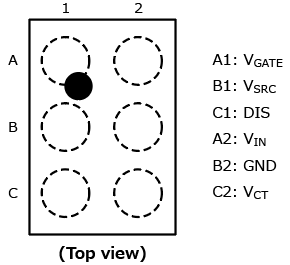
Pin Assignment
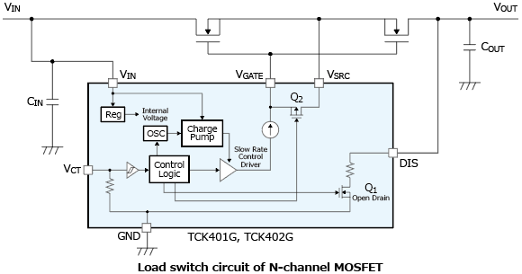
Application Circuit Example
The application circuits shown in this document are provided for reference purposes only. Thorough evaluation is required, especially at the mass-production design stage. Toshiba Electronic Devices & Storage Corporation does not grant any license to any industrial property rights by providing these examples of application circuits.
Information in this document, including product prices and specifications, content of services and contact information, is correct on the date of the announcement but is subject to change without prior notice.