Power MOSFET gate driver IPD for automotive three-phase brushless motors that helps reduce mounting size : TPD7212FN
Product News 2020-08

Toshiba Electronic Devices & Storage Corporation ("Toshiba") has launched “TPD7212FN” : Intelligent Power Device (IPD) which is a power MOSFET gate driver for automotive three-phase brushless motors.
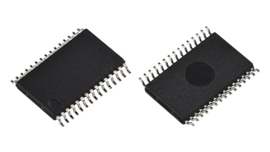
The new product “TPD7212FN” uses our latest process BiCD for integrating various analog devices and SSOP30 package[1]. Its package size was miniaturized from the conventional product “TPD7210F”[2]. The mounting area of the package is about 71 % and the height is about 80 % of the conventional product, and the pitch between pins is typical 0.65 mm. Thereby, mounting size is reduced. And it has a built-in charge pump circuit for high side N-channel power MOSFET drive, allowing a three-phase full bridge circuit to be formed easily.
The new product has extended various protection and diagnosis features, allowing it to provide feedback to systems. And it supports a wide operating temperature range (-40 °C to 150 °C) to be easily used for automotive equipment. In addition, it offers reliability conforming to AEC-Q100.
Notes :
[1] SSOP30 package : 9.7×7.6×1.2 mm (typ.)
[2] SSOP24 package : 13.0×8.0×1.5 mm (typ.)
Features
- Capable of driving the gates of power MOSFETs for three-phase brushless motors (six outputs built in)
- Built-in diagnosis features for driver power source and output terminal voltages
- AEC-Q100 qualified
Applications
Motor drivers for automotive
- Oil pumps, water pumps
- Fan motors
- Electric turbochargers
Product Specifications
(Unless otherwise specified, @Ta=25 °C)
| Part number | TPD7212FN | ||
|---|---|---|---|
| Package | Name | SSOP30 | |
| Pitch between pins typ. (mm) | 0.65 | ||
| Absolute maximum ratings |
Supply voltage (DC) VDD(DC) (V) | -0.3 to 25.0 | |
| Supply voltage (pulse) VDD (Pulse) (V) | @t≤300 ms | -0.3 to 40.0 | |
| Input voltage (EN) VEN (V) | -0.3 to 25.0 | ||
| Input voltage (IN1 to IN6) VIN (V) | -0.3 to 6.0 | ||
| Output current (Source) I×U (A) | -1.0 | ||
| Output current (Sink) I×B (A) | +1.5 | ||
| Diagnosis output voltage VDIAG (V) | -0.3 to 6.0 | ||
| Diagnosis output current IDIAG (mA) | 5 | ||
| Power dissipation PD (W) | 2.6 | ||
| Operating temperature Topr (°C) | -40 to 150 | ||
| Operating ranges |
Operating supply voltage VDD(opr) (V) | @Tj= -40 to 150 °C | 4.5 to 18.0 |
| Number of outputs | 6 | ||
| Protection function | Output judging (VDD short, GND short) |
||
| Over voltage protection (Booster) |
|||
| Diagnosis function | Output judging (VDD short, GND short) |
||
| Abnormal of the driver power supply voltage |
|||
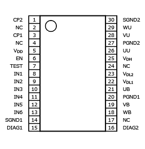
Pin Assignments

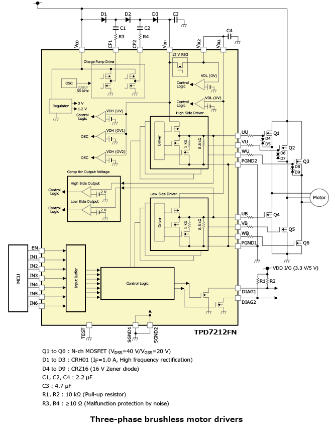
Block Diagram and Application Circuit Example

Note :
Some of the functional blocks, circuits, or constants in the block diagram may be omitted or simplified for explanatory purposes.
The application circuits shown in this document are provided for reference purposes only.
Thorough evaluation is required, especially at the mass production design stage.
Providing these application circuit examples does not grant any license for industrial property rights.
Information in this document, including product prices and specifications, content of services and contact information, is correct on the date of the announcement but is subject to change without prior notice.