
Toshiba Electronic Devices & Storage Corporation’s 300mA Small LDO Regulator ICs Combine Low Quiescent Bias Current with High Ripple Rejection Ratio and Fast Load Transient Response
September 26, 2017
Toshiba Electronic Devices & Storage Corporation
TOKYO— Toshiba Electronic Devices & Storage Corporation (TDSC) has released the “TCR3UG” series of small package, low-dropout (LDO) regulators with an output current of 300mA, that are suitable for power management of IoT modules, wearable devices and smartphones. Shipment of the first products in the series starts today, and other will follow in turn.
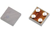
The quiescent bias current of an LDO regulator is the result of a trade-off between its ripple rejection ratio and load transient response. The TCR3UG series regulators deliver the industry’s best trade-offs between these characteristics[1]. They also deliver various protection features, such as thermal shutdown, overcurrent protection and inrush current suppression. Housed in the industry-leading small WCSP4F package[1], which measures 0.645mm x 0.645mm (typ.), t=0.33mm (max), the TCR3UG series helps reduce the size and thickness of mobile applications.
The new LDO regulators are suitable for use in sensor power supply in applications that require long battery life, and applications susceptible to noise and voltage fluctuations. The series offers 62 LDO regulators, available with 31 output voltage points, ranging from 0.8V to 5.0V, and with and without automatic output discharging, allowing easy selection for the regulator that best suits the customer’s requirements.
Applications
- IoT modules, wearable devices and smartphones
Features
- Low quiescent bias current: IB(ON1) = 0.34 μA (typ.)
- High ripple rejection ratio: R.R. = 70 dB (typ.)
- High speed load transient response: ⊿VOUT = 60 mV (typ.)
- Small WCSP4F package: 0.645 × 0.645 mm (typ.), t=0.33 mm (max)
Main Specifications
| Items (Ta=25oC) |
Auto discharge | ||
|---|---|---|---|
| Yes | No | ||
| Absolute maximum ratings | |||
| Output current IOUT(mA) | 300 | ||
| Electrical Characteristics | |||
| Input voltage VIN(V) @ IOUT = 1 mA |
1.5 to 5.5 | ||
| Quiescent current IB(ON1) typ. (μA) @ VOUT ≦ 1.5 V, IOUT=0 mA *2 |
0.34 | ||
| Ripple rejection ratio R.R. typ. (dB) @VOUT=0.8 V, IOUT=10 mA, f=1 kHz *2 |
70 | ||
| Drop-out voltage VIN-VOUT typ. (mV) @ VOUT=3.3 V, IOUT=300 mA |
140 | ||
| Load transient response ⊿VOUT typ. (mV) @VOUT=0.8 V, VIN=3.3 V, IOUT=1mA⇔50 mA *2 |
±60 | ||
Lineup
Output voltage typ. |
Auto discharge | Output voltage typ. |
Auto discharge | ||
|---|---|---|---|---|---|
| Yes | No | Yes | No | ||
| 0.8 | 2.5 | ||||
| 0.85 | 2.6 | ||||
| 0.9 | 2.7 | ||||
| 0.95 | 2.8 | ||||
| 1.0 | 2.85 |
||||
| 1.05 | 3.0 | ||||
| 1.1 | 3.1 | ||||
| 1.15 | 3.2 | ||||
| 1.2 | 3.3 | ||||
| 1.3 | 3.5 | ||||
| 1.35 | 3.6 | ||||
| 1.5 | 4.1 | ||||
| 1.75 | 4.2 | ||||
| 1.8 | 4.5 | ||||
| 1.85 | 5.0 | ||||
| 1.9 | |||||
Notes:
[1] As of September 26, 2017 for LDO regulator ICs with an output current of 300mA. TDSC survey.
[2] Common test conditions: VIN = VOUT + 1 V (VOUT > 1.5 V), VIN = 2.5 V (VOUT ≤ 1.5 V), CIN=1.0 μF, COUT=1.0 μF (unless otherwise noted)
Follow the link below for more on TDSC’s LDO Regulators line-up.
Customer Inquiries:
Small Signal Device Sales & Marketing Department
Tel: +81-3-3457-3411
*Information in this document, including product prices and specifications, content of services and contact information, is current on the date of the announcement but is subject to change without prior notice.