
A MOSFET gate driver switch IPD for automotive high current applications : TPD7106F
Product News 2020-05
Toshiba Electronic Devices & Storage Corporation (“Toshiba”) has launched “TPD7106F”: a gate driver switch IPD[1] that controls conduction and shut-off of current that is supplied for automotive Electronic Control Units (ECUs) such as junction boxes and body control modules.
The new product can form a high-side switch supporting high current application in combination with Toshiba’s automotive low On-resistance N-channel MOSFET[2]. Unlike mechanical relays, the switch does not have contact wear, so it makes devices maintenance-free.
In order to protect MOSFETs in the event of short-circuit, there is an input/output terminal to turn off MOSFETs rapidly, and it can be controlled independently from micro-controllers. It turns MOSFETs off against unusual operation.
Furthermore, it has 150 °C of high operating temperature rating, and enables operating under high temperature environment. The leakage current is suppressed in case of reversed battery connection, and it supports source common connection of MOSFETs. It features low stand-by current, maximum 5 μA.
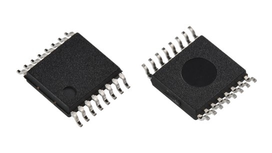
And it uses small SSOP16[3] package and this contributes to downsizing and low-power-consumption of automotive ECUs.
Notes :
[1] IPD (Intelligent Power Device)
[2] Example of use devices : TKR74F04PBx4 (40 V/250 A)
[3] SSOP16 : 5.0×6.4 mm (typ.)
Features
- AEC-Q100 qualified
- Can be used in combination with a low On-resistance N-channel MOSFET[2] depending on the load current
- Built in the input/output terminal for MOSFET rapid turn-off against unusual operation
Applications
Automotive equipment
- ECUs (Body control modules and junction boxes, etc.)
- Power distribution modules
- Semiconductor relays
Product Specifications
(Unless otherwise specified, @Ta=25 °C)
| Part number | TPD7106F | ||
|---|---|---|---|
| Package | SSOP16 | ||
| Absolute maximum ratings |
Supply voltage VDD(1) (V) | -18 to 27 | |
| Supply voltage VDD(2) (V) | @t≤500 ms | 40 | |
| Input voltage VSTBY (V) | -0.3 to 40.0 | ||
| Input voltage VIN(1), VIN(2) (V) | -0.3 to 6.0 | ||
| CPV voltage VCPV (V) | 40 | ||
| TEST pin voltage VTEST (V) | 40 | ||
| Output source current IOUT1(1) (mA) | -10 | ||
| Output sink current IOUT1(2) (mA) | 10 | ||
| Output sink current IOUT2 (mA) | 400 | ||
| DIAG Output voltage VDIAG (V) | -0.3 to 40.0 | ||
| DIAG Output current IDIAG (mA) | 5 | ||
| Power dissipation PD (W) | 1.16 | ||
| Operating temperature Topr (°C) | -40 to 150 | ||
| Operating ranges |
Operating supply voltage VDD (V) | @Tj= -40 to 150 °C | 4.5 to 27.0 |
| Electrical characteristics |
Rapid off drive operation time tO2ON typ. (μs) | @Tj=25 °C | 100 |
| Supply current IDD(1) max (μA) | @standby, Tj=25 °C | 5.0 | |
Block Diagram
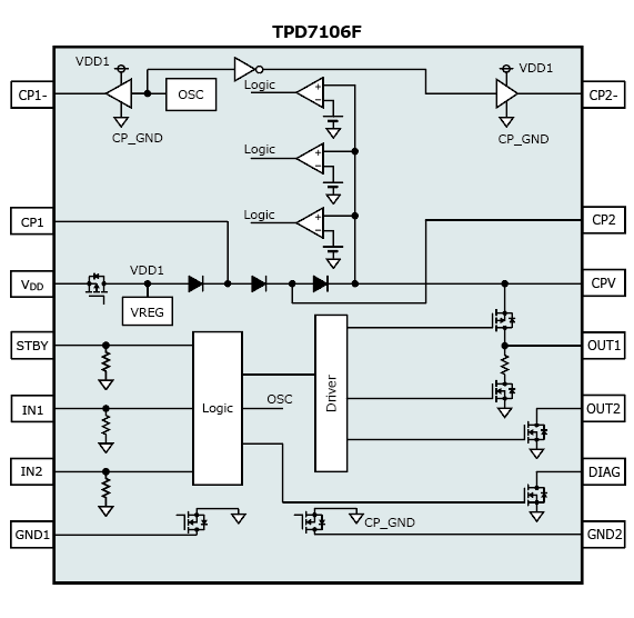
Note : Some of the functional blocks, circuits, or constants in the block diagram may be omitted or simplified for explanatory purposes.
Example of Application Circuit
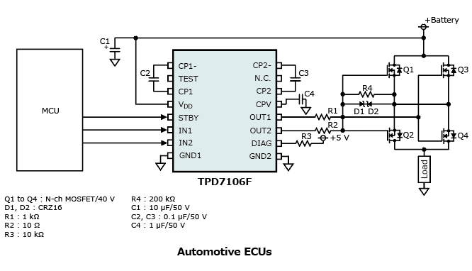
Note : The application circuits shown in this document are provided for reference purposes only. Thorough evaluation is required, especially at the mass production design stage. Providing these application circuit examples does not grant any license for industrial property rights.
Information in this document, including product prices and specifications, content of services and contact information, is correct on the date of the announcement but is subject to change without prior notice.