Toshiba Launches Photocoupler with Built-in Protective Functions for Medium to High Current IGBT/MOSFET
March 10, 2020
Toshiba Electronic Devices & Storage Corporation

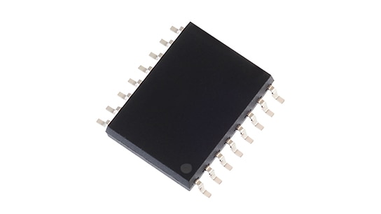
TOKYO—Toshiba Electronic Devices & Storage Corporation (“Toshiba”) has introduced “TLP5231,” a pre-drive photocoupler for medium to high current insulated gate bipolar transistor (IGBT) and MOSFET, for industrial inverters and photovoltaic (PV) power conditioning systems. The new pre-drive photocoupler delivers various built-in functions[1], including an overcurrent detection by monitoring collector voltage. Shipments start today.
The new pre-drive photocoupler controls the gates of medium to high current IGBT and MOSFET by using external p-channel and n-channel complementary MOSFET as buffers.
Current products[2] require the use of buffer circuits composed of bipolar transistors for current amplification, which consume base current during operation. The new product eanbles use of external complementary MOSFET buffers, limiting current consumption to during charge or discharge of the buffer MOSFET gate, which reduces power consumption.
By changing external complementary MOSFET buffer sizes, the TLP5231 can produce required gate currents for various IGBT and MOSFET. A configuration of the TLP5231, the MOSFET buffer, and the IGBT and MOSFET can be used as platforms to cover the power requirements of systems, contributing to the easier design.
Other features include control of “gate soft turn-off time” with another external n-channel MOSFET after VCE(sat) overcurrent detection, and, in addition to VCE(sat) overcurrent detection by monitoring the collector voltage, UVLO[3] detection that outputs any fault signal to the primary side. These new features, not found in current products[2], make it easier for users to design gate drive circuits.
Applications
- IGBT and power MOSFET gate drivers (pre-drivers)
- AC and brushless DC motor control
- Industrial inverters and uninterruptible power supplies (UPS)
- Photovoltaic (PV) power conditioning systems
Features
- Dual outputs with built-in active timing control, suitable for driving p-channel and n-channel complementary-MOSFET buffers
- Configurable gate soft turn-off time using another external n-channel MOSFET when overcurrent is detected.
- Fault signals are output on the primary side when overcurrent is detected by monitoring collector voltage, or when an UVLO is detected.
Main Specifications
(Unless otherwise specified, @Ta = -40 to 110°C.)
Part number |
||
|---|---|---|
Absolute maximum ratings |
Peak high-level output current IOPH (A) |
-2.5 |
Peak low-level output current IOPL (A) |
+2.5 |
|
Electrical characteristics |
VOUTP high level output current IOUTPH max (A) |
-1.0 |
VOUTP low level output current IOUTPL min (A) |
1.0 |
|
VOUTN high level output current IOUTNH max (A) |
-1.0 |
|
VOUTN low level output current IOUTNL min (A) |
1.0 |
|
High level supply current (VCC2) ICC2H max (mA) |
10.2 |
|
Low level supply current (VCC2) ICC2L max (mA) |
10.2 |
|
High level supply current (VEE) IEEH min (mA) |
-9.2 |
|
Low level supply current (VEE) IEEL min (mA) |
-9.2 |
|
Threshold input current (H/L) IFHL max (mA) |
3.5 |
|
Recommended operating conditions |
Total output supply voltage (VCC2-VEE) (V) |
21.5 to 30 |
Negative output supply voltage (VE-VEE) (V) |
-15 to -6.5 |
|
Positive output supply voltage (VCC2-VE) (V) |
15 to 23.5 |
|
Switching characteristics
|
Propagation delay time (L/H) tpLH (ns) |
100 to 300 |
Propagation delay time (H/L) tpHL (ns) |
100 to 300 |
|
Propagation delay skew(device to device) tpsk (ns) |
-200 to 200 |
|
High-level common-mode transient immunity CMH min (kV/μs) |
±25 |
|
Low-level common-mode transient immunity CML min (kV/μs) |
±25 |
|
Function |
Protection function |
IGBT VCE(sat) detection, UVLO[4] |
Feedback (FAULT): Activates when VCE(sat) detecton, UVLO detection (open-collector output) |
||
Isolation characteristic (@Ta = 25°C) |
Isolation voltage BVS min (Vrms) |
5000 |
Mechanical |
Clearance distances min (mm) |
8.0 |
Creepage disances min (mm) |
8.0 |
|
Internal isolation thickness min (mm) |
0.4 |
|
Stock Check & Purchase |
||
Notes:
[1] Gate signal soft turn off, fault feedback function
[2] TLP5214, TLP5214A
[3] UVLO: Under voltage lockout
[4] Common at VE
Follow the link below for more on the new product.
Follow the link below for more on Toshiba’s optical devices line-up.
*Company names, product names, and service names may be trademarks of their respective companies.
Customer Inquiries
Optoelectronic Device Sales & Marketing Dept.
Tel: +81-3-3457-3431
Information in this document, including product prices and specifications, content of services and contact information, is current on the date of the announcement but is subject to change without prior notice.
