
Toshiba Develops Technology that Can Mitigate Parasitic Oscillation Between Parallel-Connected Chips in SiC Power Modules with Minimal Gate Resistance that Support High Speed Switching
July 26, 2024
Toshiba Electronic Devices & Storage Corporation
Toshiba Corporation
Toshiba Electronic Devices & Storage Corporation and Toshiba Corporation (Toshiba Group) have developed technology that mitigates the parasitic oscillation[1] that occurs during switching operations by power modules with silicon carbide (SiC) MOSFETs[2] connected in parallel, even with a 60% smaller gate resistance[3][4] than is typical. The technology reduces power loss in power modules, mitigates oscillation, and realizes highly reliable switching operations.
The drive for carbon neutrality is stimulating demand for technologies that improve energy efficiency in many areas, including renewables, railways, and industrial equipment. In these sectors, the application of power modules built around SiC MOSFETs is seen as a solution that supports high-speed switching at high voltages and large currents—which is particularly important for the miniaturization of power converters, where higher switching frequencies result in higher rates of switching losses against power consumption.
Connecting multiple chips in parallel in power modules can form oscillation circuits, the result of wiring inductance[5] between the chips and their parasitic capacitance[6]. It can reduce module reliability if not countered, which is usually done by increasing gate resistance. However, this approach slows switching speed, resulting in a trade-off with switching losses. For power modules with SiC MOSFETs to perform high-speed switching, another approach is needed.
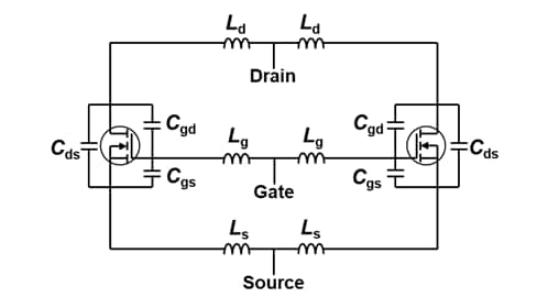
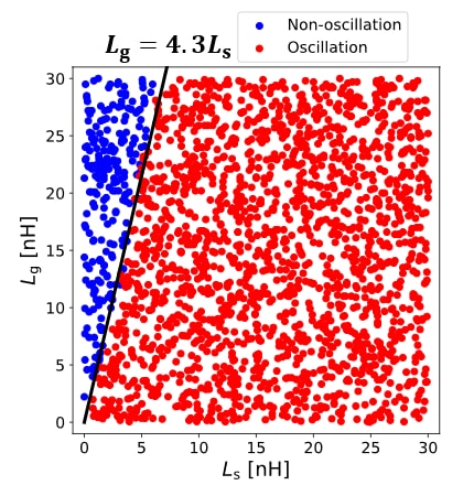
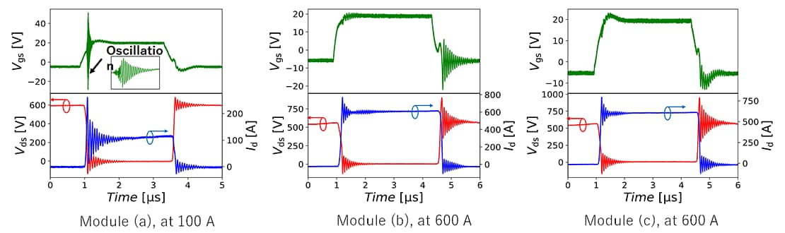
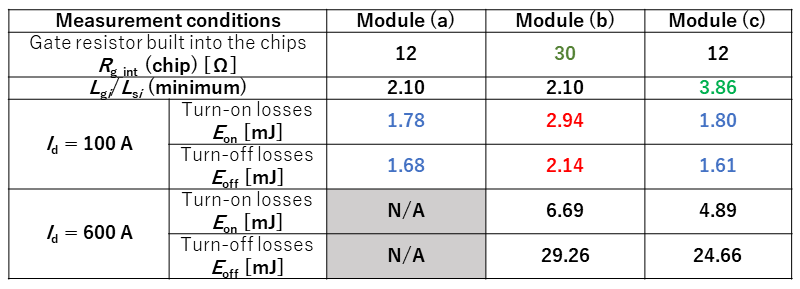
Toshiba Group used an equivalent circuit model of the power module (Figure 1) to determine the theoretical condition that triggers parasitic oscillation, and developed a wiring layout less likely to cause it. This was done by analyzing simulations of parasitic oscillation occurs when Lg/Ls, the ratio of gate-to-gate inductance Lg and source-to-source inductance Ls of parallel chips, is below a certain value (Figure 2). As increasing Lg/Ls is an effective means of mitigating parasitic oscillation, Toshiba Group fabricated prototype modules with different Lg/Ls and measured switching. This confirmed that increasing Lg/Ls mitigated oscillation, even with a 60% smaller gate resistance than that required by the alternative approach of increasing gate resistance (Figure 3).
Applying this approach to oscillation mitigation in power modules now under development has realized a power module less likely to cause parasitic oscillation, even with minimal gate resistance, that achieves low power loss with mitigated oscillation, and delivers highly reliable switching operation. Toshiba Group will continue to make refine the modules toward an early product launch. Toshiba Group presented the details of this technology on June 6 at the 36th International Symposium on Power Semiconductor Devices and ICs (ISPSD) 2024, an international power semiconductor conference held in Bremen, Germany from June 2 to 6.
[1] Parasitic oscillation: Gate voltage oscillation that occurs during switching by MOSFETs. It is more likely to occur when multiple MOSFETs are used in parallel.
[2] MOSFET: Metal Oxide Semiconductor Field Effect Transistor, a switching device with three electrodes: gate, drain, and source. Current between the drain and source is switched on and off by applying a gate voltage.
[3] Comparison with conventional Toshiba products
[4] Gate resistance: Resistance in the MOSFET gate that limits current flow when gate voltage is applied. Its value is an important factor in determining device switching characteristics and signal rise time.
[5] Wiring inductance: An inherent operating characteristic of conductors: resistance to changes in electric current flows. It is due the electromotive force (voltage) induced in opposition to the current change due to the magnetic field created around the conductor.
[6] Parasitic capacitance: Unwanted capacitance between components or wiring in electronic circuits. It can store an electric charge, like a capacitor, that can affect circuit operation. In high speed circuits, it can cause signal delays and distortions.
Vgs: Gate-Source voltage, Vds: Drain-Source voltage, Id: Drain current
* Company names, product names, and service names may be trademarks of their respective companies.
* Information in this document, including product prices and specifications, content of services and contact information, is current on the date of the announcement but is subject to change without prior notice.