- 型號查詢
- 交叉搜尋
- 關鍵字搜尋
- 參數搜尋
- 線上庫存查詢跟購買
This webpage doesn't work with Internet Explorer. Please use the latest version of Google Chrome, Microsoft Edge, Mozilla Firefox or Safari.
型號需要超過三個文字以上
The information presented in this cross reference is based on TOSHIBA's selection criteria and should be treated as a suggestion only. Please carefully review the latest versions of all relevant information on the TOSHIBA products, including without limitation data sheets and validate all operating parameters of the TOSHIBA products to ensure that the suggested TOSHIBA products are truly compatible with your design and application.
Please note that this cross reference is based on TOSHIBA's estimate of compatibility with other manufacturers' products, based on other manufacturers' published data, at the time the data was collected.
TOSHIBA is not responsible for any incorrect or incomplete information. Information is subject to change at any time without notice.
型號需要超過三個文字以上
Board design considerations for TVS diodes (ESD protection diodes)
Even TVS diodes with high ESD protection performance do not provide sufficient ESD protection without adequate board design. In particular, board design affects the instantaneous high-frequency pulse that occurs upon ESD entry.
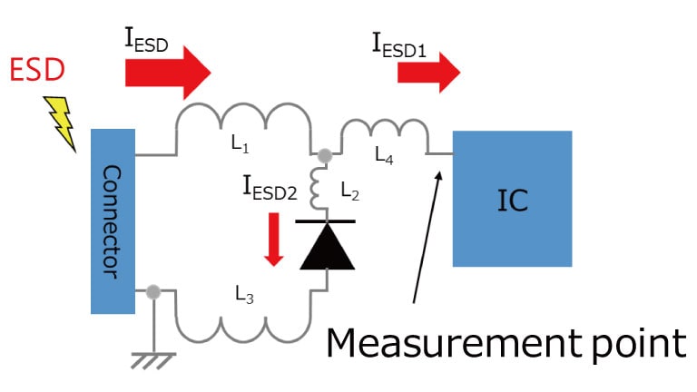
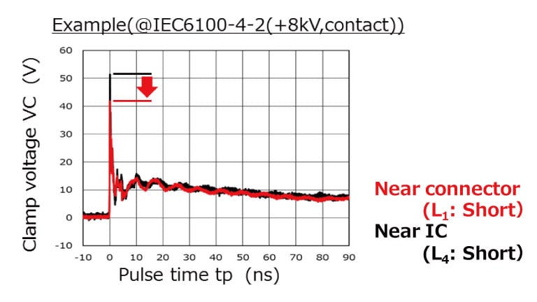
The following figure compares the clamp voltage waveforms, depending on the distance of a TVS diode from a connector, and the ESD entry point. As can be seen from this figure, when a TVS diode is placed close to the connector (i.e., far from the IC under protection), the first peak voltage (i.e., the voltage immediately after ESD entry) is nearly 10 V lower than the case in which it is placed close to the IC.
The following considerations apply to board design:
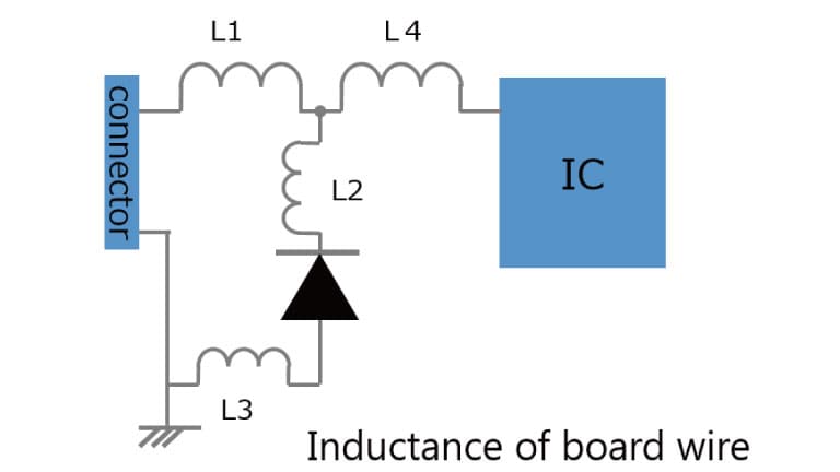
- Place a TVS diode as close as possible to the connector (to minimize the length of the L1 trace).
- Reduce the lengths of L2 and L3 following the TVS diode.
- Do not use via holes (through-holes) in the L2 and L3 traces.
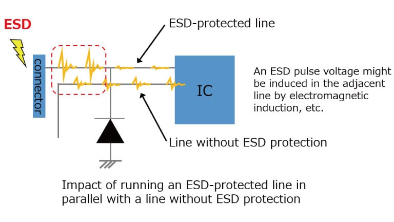
- Do not run ESD-protected lines connected to an ESD entry point in parallel with lines that are not protected from ESD. These lines should not run in parallel particularly from the ESD entry point to the TVS diode.