Lineup Expansion of Digital Isolators that Contribute to Stable High-Speed Isolated Data Transmissions in Industrial Applications
Product News 2023-11

Toshiba Electronic Devices & Storage Corporation ("Toshiba") has expanded the lineup with the addition of four products to DCL54xx01 Series of quad-channel digital isolators with high common mode transient immunity (CMTI) and high-speed data rate.
The enabling control is possible by the output enable terminal[1].
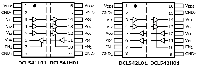
The channel configuration of "DCL541H01 and DCL541L01" is three channel of forward directions and one channel of reverse direction and that of "DCL542H01 and DCL542L01" is two channel of forward directions and two channel of reverse directions. The lineup of ten products including six products of precedence release products offers the selection of enabled control and channel configuration widely.
DCL54xx01 Series use Toshiba's proprietary magnetic coupling type insulated transmission method to deliver a high CMTI of 100 kV/μs (min)[2].This provides high tolerance of electrical noise between input/output in isolated signal communications, and contributes to stable control signal transmission and equipment operation. With their low pulse width distortion of 0.8 ns (typ.)[3] and high-speed data rate of 150 Mbps (max), the digital isolators are suitable for multi-channel high-speed communications applications such as I/O interfaces with SPI communication.
Notes:
[1] The output is enabled by the enable control signal High. Conversely, the output is disabled (output high impedance) by the enable control signal Low.
[2] Test condition: VI=VDDI or 0 V, VCM=1500 V, Ta=25 °C
[3] Test condition: VDD1=VDD2=5 V, Ta=25 °C
Applications
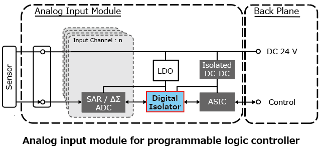
- Industrial automation systems (programmable logic controllers, I/O interfaces, etc.)
- Motor control
- Inverters
Features
- The enabling control is possible by the output enable terminal[1].
- Quad-channel:
Three channel of forward directions and one channel of reverse direction
Two channel of forward directions and two channel of reverse directions - High common mode transient immunity: CMTI=100 kV/μs (min)[2]
Main Specifications
| Part number | DCL541L01 | DCL541H01 | DCL542L01 | DCL542H01 | |||
|---|---|---|---|---|---|---|---|
| Number of channels (Forward directions : reverse directions) |
4 (3:1) |
4 (3:1) |
4 (2:2) |
4 (2:2) |
|||
| Default output logic | Low | High | Low | High | |||
| Enabled control | Output enable | ||||||
| Package | SOIC16-W | ||||||
| Absolute maximum ratings |
Operating temperature Topr (°C) | -40 to 110 | |||||
| Storage temperature TSTG (°C) | -65 to 150 | ||||||
| Maximum withstanding isolation voltage (1 min.) BVS (Vrms) |
Ta=25 °C | Min | 5000 | ||||
| Recommended operating conditions |
Power supply voltage VDD1, VDD2 (V) |
Topr=-40 °C to 110 °C |
2.25 to 5.5 | ||||
| Electrical characteristics |
Common mode transient immunity CMTI (kV/μs) |
Ta=25 °C | Min | 100 | |||
| Data rate tbps (Mbps) |
Ta=-40 °C to 110 °C |
Max | 150 | ||||
| Pulse width distortion PWD (ns) |
VDD1=VDD2=5 V, Ta=25 °C |
Typ. | 0.8 | ||||
| Propagation delay tPHL, tPLH (ns) |
Typ. | 10.9 | |||||
Pin Assignments

Application Circuit Example

Note:
The application circuits shown in this document are provided for reference purposes only.
Thorough evaluation is required, especially at the mass-production design stage.
Providing these application circuit examples does not grant any license for industrial property rights.
* Company names, product names, and service names may be trademarks of their respective companies.
* Information in this document, including product prices and specifications, content of services and contact information, is current on the date of the announcement but is subject to change without prior notice.