Lineup Expansion of 150V N-Channel Power MOSFETs Using a New Generation Process that Helps Reduce Power Consumption of Power Supplies
Product News 2024-10

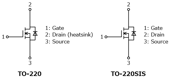
Toshiba Electronic Devices & Storage Corporation ("Toshiba") has expanded the lineup of 150V N-channel power MOSFETs with new six products that use the new generation process “U-MOSⅩ-H series.” Products in this series are suitable for the switching power supplies of industrial equipment such as data centers and communication base. The package of new products is a three-pin through hole type: TO-220 for "TK4R9E15Q5, TK7R2E15Q5 and TK9R6E15Q5" and TO-220SIS for "TK5R0A15Q5, TK7R4A15Q5 and TK9R7A15Q5."
The new products use the U-MOSⅩ-H process to achieve low drain-source On-resistance. In particular, TK4R9E15Q5 features the excellent low drain-source On-resistance of 4.9mΩ (max). In addition, the new products uses high-speed diode (HSD) to improve reverse recovery characteristics[1], which are important for synchronous rectification applications, by reducing reverse recovery charge and faster reverse recovery time. Used in synchronous rectification applications, the new products reduce the power loss of switching power supplies and help improve efficiency.
The first product TPH9R00CQ5[2] which uses HSD, has approximately 74% less reverse recovery charge and approximately 44% faster reverse recovery time than Toshiba‘s existing product TPH9R00CQH[2], which does not use HSD. The U-MOSⅩ-H process using this HSD has applied to through hole type packages in addition to surface mount type packages.
The new products have reduced the drain source spike voltage[3] generated between the drain and source when MOSFET is switching, helping to lower EMI in switching power supplies.
Toshiba will continue to promote the expansion of its power MOSFET lineup, which helps improve the efficiency of power supplies, thereby contributing to reducing the power consumption of equipment.
Notes:
[1] A switching action in which the MOSFET body diode switches from forward to reverse biased
[2] SOP Advance/SOP Advance(N) package products
[3] When used in a circuit that operates in reverse recovery mode
Applications
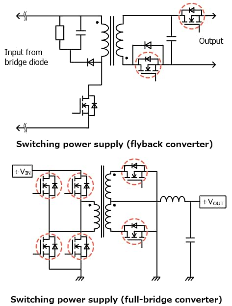
- Switching power supplies for communication equipment, etc. (high efficiency AC-DC converters, high efficiency DC-DC converters, etc.)
- Motor control equipment (motor drives, etc.)
Features
- Excellent low On-resistance:
TK4R9E15Q5 RDS(ON)=4.9mΩ (max) (VGS=10V) - Low reverse recovery charge:
TK9R6E15Q5 Qrr=32nC (typ.) (-dIDR/dt=100A/μs) - Fast reverse recovery time:
TK9R6E15Q5 trr=40ns (typ.) (-dIDR/dt=100A/μs)
Main Specifications
(Ta=25°C unless otherwise specified)
| Part number | Absolute maximum ratings | Electrical characteristics | Packages | ||||||||
|---|---|---|---|---|---|---|---|---|---|---|---|
| Drain- source voltage VDSS (V) |
Drain current (DC) ID (A) |
Channel temperature Tch (°C) |
Drain-source On-resistance RDS(ON) (mΩ) |
Total gate charge Qg (nC) |
Input capacitance Ciss (pF) |
Gate resistance rg (Ω) |
Reverse recovery time trr (ns) |
Reverse recovery charge Qrr (nC) |
|||
| VGS= 10V |
VGS= 8V |
-dIDR/dt= 100A/μs |
|||||||||
| Tc= 25°C |
Max | Max | Typ. | Typ. | Typ. | Typ. | Typ. | ||||
| TK4R9E15Q5 | 150 | 120 | 175 | 4.9 | 5.9 | 96 | 7820 | 1.9 | 50 | 50 | TO-220 |
| TK7R2E15Q5 | 84 | 7.2 | 8.7 | 66 | 4970 | 1.7 | 44 | 42 | |||
| TK9R6E15Q5 | 52 | 9.6 | 11.5 | 50 | 3690 | 1.6 | 40 | 32 | |||
| TK5R0A15Q5 | 76 | 5 | 6 | 96 | 7820 | 1.9 | 52 | 55 | TO-220SIS | ||
| TK7R4A15Q5 | 57 | 7.4 | 8.8 | 66 | 4970 | 1.7 | 44 | 40 | |||
| TK9R7A15Q5 | 49 | 9.7 | 11.6 | 50 | 3690 | 1.5 | 40 | 32 | |||
Internal Circuits

Application Circuit Examples

Note:
The application circuits shown in this document are provided for reference purposes only.
Thorough evaluation is required, especially at the mass production design stage.
Providing these application circuit examples does not grant any license for industrial property rights.
* Company names, product names, and service names may be trademarks of their respective companies.
* Information in this document, including product prices and specifications, content of services and contact information, is current on the date of the announcement but is subject to change without prior notice.