Toshiba Opens the Way to Longer Life Wearables and IoT Devices with New IC Chips
January 13, 2022
Toshiba Electronic Devices & Storage Corporation

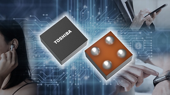
KAWASAKI, Japan—Toshiba Electronic Devices & Storage Corporation ("Toshiba") has brought to market the “TCK12xBG Series” of load switch ICs that deliver a remarkable decrease in quiescent current[1] and an output current rating of 1A. Housed in a small WCSP4G package, the new ICs will support product developers in innovating a new generation of wearables and IoT devices that consume less power and offer a longer charge life. Volume shipments start today.
TCK12xBG Series uses a new driver circuit, which realizes a typical ON-state quiescent current of 0.08nA[1]. This represents in the region of 99.9% reduction from Toshiba’s current product, “TCK107AG,” a huge advance in efficiency that will allow wearables and IoT devices powered by small batteries to operate for significantly longer.
WCSP4G, a new package developed for the products, is about 34% smaller than that of TCK107AG, only 0.645×0.645mm, which allows mounting on small boards. Its back coating can reduce the damage that can happen to such a minute chip in the mounting process.
Toshiba has prepared a line-up of three ICs: TCK127BG with automatic discharge that turns on at active high; TCK126BG without automatic discharge that turns on at active high; and TCK128BG with automatic discharge that turns on at active low. This offers product developers and designers the freedom to select the load switch IC that best suits their design requirement.
Toshiba will continue to enhance low quiescent current technology products, to contribute to equipment downsizing and lower power consumption, and to a sustainable future.
Applications
- Wearables, IoT devices, smartphones (ON and OFF switch of power supply for sensors, etc.)
- Replacement of load switch circuits formed by discrete semiconductors such as MOSFETs, transistors, etc.
Features
- Ultra-low quiescent current (ON state)[1]: IQ=0.08nA (typ.)
- Low standby current (OFF state): IQ(OFF)+ISD(OFF)=13nA (typ.)
- Compact WCSP4G package: 0.645×0.645mm (typ.), t:0.465mm (max.)
- Backside coating that reduces damage in board-mounting process
Note:
[1] Among load switch ICs with a compact package size of 1mm2 or less and an output current rating of 1A. Toshiba survey, as of January 2022.
Main Specifications
(Unless otherwise specified, @Ta=25°C)
Part number |
|||||
|---|---|---|---|---|---|
Package |
Name |
WCSP4G |
|||
Size typ. (mm) |
0.645x0.645, t:0.465 (max) |
||||
Absolute maximum ratings |
Input voltage VIN (V) |
-0.3 to 6.0 |
|||
Control voltage VCT (V) |
-0.3 to 6.0 |
||||
Output current IOUT (A) |
DC | 1.0 |
|||
| Pulse | 2.0 |
||||
Power dissipation PD (W) |
1.0 | ||||
Operating ranges (@Ta_opr= -40 to 85°C) |
Input voltage VIN (V) |
1.0 to 5.5 |
|||
Output current IOUT max (A) |
1.0 |
||||
Electrical characteristics |
Quiescent current IQ typ. (nA) |
@VIN=5.5V |
0.08 |
||
Standby current IQ(OFF) + ISD(OFF) typ. (nA) |
@VIN=5.5V |
13 |
|||
On-resistance |
@VIN=5.0V, IOUT= -0.5A |
46 |
|||
@VIN=3.3V, IOUT= -0.5A |
58 |
||||
@VIN=1.8V, IOUT= -0.5A |
106 |
||||
@VIN=1.2V, IOUT= -0.2A |
210 |
||||
@VIN=1.0V, IOUT= -0.05A |
343 |
||||
AC characteristics |
VOUT rise time tr typ. (μs) |
@VIN=3.3V |
363 |
363 |
363 |
VOUT fall time tf typ. (μs) |
125 |
32 |
32 |
||
Turn on delay tON typ. (μs) |
324 |
324 |
324 |
||
Turn off delay tOFF typ. (μs) |
10 |
10 |
10 |
||
Auto-discharge function |
- |
Built-in |
Built-in |
||
ON/OFF control logic |
Active High |
Active High |
Active Low |
||
Sample Check & Availability |
|||||
Follow the links below for more on the new product.
TCK126BG
TCK127BG
TCK128BG
Follow the link below for more on Toshiba’s Load Switch ICs.
Load Switch ICs
To check availability of the new products at online distributors, visit:
Customer Inquiries
Small Signal Device Sales & Marketing Dept.
Tel: +81-44-548-2215
* Company names, product names, and service names may be trademarks of their respective companies.
* Information in this document, including product prices and specifications, content of services and contact information, is current on the date of the announcement but is subject to change without prior notice.
