Toshiba Launches 30V N-Channel Common-Drain MOSFET Suitable for Devices with USB and for Protecting Battery Packs
November 7, 2023
Toshiba Electronic Devices & Storage Corporation

KAWASAKI, Japan—Toshiba Electronic Devices & Storage Corporation ("Toshiba") has launched “SSM10N961L,” a low on-resistance, 30V N-channel common-drain MOSFET, suitable for devices with USB and for protecting battery packs. Shipments start today.
Until now, Toshiba’s line-up of N-channel common-drain MOSFETs has focused on 12V products, mainly for use in protecting the lithium-ion battery packs of smartphones. The release of a 30V product realizes a wider selection of applications requiring voltages higher than 12V, such as load switching for the power lines of USB charging devices, and the protection of lithium-ion battery packs in laptop PCs and tablets.
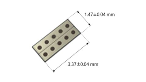
Realizing a bi-directional switch with a low drain-source on-resistance (RDS(ON)) has required two MOSFETs, either 3.3×3.3mm or 2×2 mm, with low RDS(ON). Toshiba’s new product uses a new, small, thin package TCSPAG-341501 (3.37mm×1.47mm (typ.), t=0.11mm (typ.)), and features low source-source on-resistance (RSS(ON)) of 9.9mΩ (typ.) in a single package common-drain configuration
USB Power Delivery (USB PD) that supports a power supply ranging 15W (5V / 3A) to a maximum of 240W (48V / 5A) was developed for devices requiring high power supply. USB PD specifies a role swap function for swapping the power supply and receiving side, and requires devices with USB charging to support bi-directional power supply, so that both sides can supply and receive power. The new product is an N-channel common-drain MOSFET that supports bi-directional power supply, and that has a small mounting area.
Combining the product with a driver IC in Toshiba’s TCK42xG series forms a load switching circuit with a backflow prevention function or a power multiplexer circuit that can switch operations between Make-Before-Break (MBB) and Break-Before-Make (BBM). Toshiba has today released a reference design for a power multiplexer circuit (using common-drain MOSFETs) based on this product combination. Use of the reference design will help to reduce product design and development times.
Toshiba will continue to expand its product line-up and improve characteristics, to raise design flexibility.


Applications
- Smartphones
- Laptop PCs
- Tablets, etc.
Features
- High source-source voltage rating: VSSS=30V
- Low on-resistance: RSS(ON)=9.9mΩ (typ.) (VGS=10V)
- Common‐drain connection structure for bi-directional conduction
- Small and thin type TCSPAG-341501 package: 3.37mm×1.47mm (typ.), t=0.11mm (typ.)
Main Specifications
(Unless otherwise specified, Ta=25°C)
| Part number | SSM10N961L | |||
|---|---|---|---|---|
| Polarity | N-channel×2 | |||
| Internal connection | Common-drain | |||
| Absolute maximum ratings |
Source-source voltage VSSS (V) | 30 | ||
| Gate-source voltage VGSS (V) | ±20 | |||
| Source current (DC) IS (A)[1] | 9.0 | |||
| Source current (DC) IS (A)[2] | 14.0 | |||
| Electrical characteristics |
Source-source breakdown voltage V(BR)SSS (V) | VGS=0V | Min | 30 |
| Source–source on-resistance RSS(ON) (mΩ) | VGS=10V | Typ. | 9.9 | |
| VGS=4.5V | Typ. | 13.6 | ||
| Package | Name | TCSPAG-341501 | ||
| Size (mm) | Typ. | 3.37×1.47, t=0.11 | ||
| Sample Check & Availability |  |
|||
Notes:
[1] Device mounted on a 25mm×27.5mm, t=1.6mm, Cu Pad: 18µm, 407mm2, FR4 glass epoxy board
[2] Device mounted on a 25mm×27.5mm, t=1.6mm, Cu Pad: 70µm, 687.5mm2, FR4 glass epoxy board
Follow the link below for more on the new product.
Follow the link below for more on Toshiba’s MOSFETs.
Follow the links below for more on Toshiba’s solution proposals using the new product.
Application
Smart Watch
Action Camera
Tablet Device
Customer Inquiries:
Small Signal Device Sales & Marketing Dept.
Tel: +81-44-548-2215
* Company names, product names, and service names may be trademarks of their respective companies.
* Information in this document, including product prices and specifications, content of services and contact information, is current on the date of the announcement but is subject to change without prior notice.