
Product News 2020-10
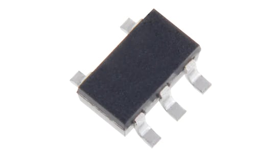
Toshiba Electronic Devices & Storage Corporation (“Toshiba”) has commercialized and has expanded our line-up with the launch of “TC75S103F,” a low consumption current, input and output full range CMOS operational amplifier suitable for various sensors[1] of mobile devices[2].
The new product features a typical supply current as low as 100 μA, which helps to reduce the power consumption of the device and drive the mobile device[2] for long periods of time. The new product features input and output full range (input and output Rail-to-Rail) and the minimum supply voltage is 1.8 V, enabling low voltage drive. In addition, the maximum input offset voltage is as low as 1.5 mV, which contributes to improving sensibility of sensor.
Demand for operational amplifier with low consumption and low voltage drive is increasing due to the increased number of IoT equipment and the use of a wide variety of sensors[1] in mobile devices[2]. To meet these requirements, we have developed this product onto our lineup.
Features
- Low supply current : IDD=100 μA (typ.) @VDD=1.8 V
- Input and output full range (Input and output Rail-to-Rail)
- Low operating voltage range : VDD-VSS=1.8 V (min)
- Low input offset voltage : VIO=1.5 mV (max) @VDD=1.8 V
Applications
- Various sensors[1] of mobile devices[2]
- IoT equipments
- Consumer equipments
Product Specifications
(Unless otherwise specified, @Ta=25 °C)
| Part number |
Package name (Package code) |
Operating ranges |
Electrical characteristics | |||||
|---|---|---|---|---|---|---|---|---|
| Supply voltage VDD-VSS @Ta=-40 to 105 °C (V) |
Supply current IDD @VDD=1.8 V (μA) |
Input offset voltage VIO max @VDD=1.8 V (mV) |
Source current Isource typ. @VDD=1.8 V (mA) |
Sink current Isink typ. @VDD=1.8 V (mA) |
Unity gain cross frequency fT typ. @VDD=0.9 V, VSS=-0.9 V (MHz) |
|||
| typ. | max | |||||||
| TC75S103F | SMV (SOT-25) |
1.8 to 5.5 | 100 | 165 | 1.5 | 2 | 2 | 0.3 |
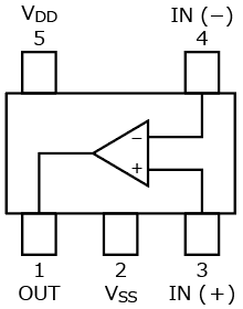
Pin Assignment (top view)
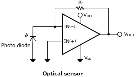
Application Circuit Example
The application circuits shown in this document are provided for reference purposes only.
Thorough evaluation is required, especially at the mass production design stage.
Providing these application circuit examples does not grant any license for industrial property rights.
Information in this document, including product prices and specifications, content of services and contact information, is correct on the date of the announcement but is subject to change without prior notice.