
Toshiba Announces 13 Mega Pixel, 1.12 Micrometer, CMOS Image Sensor With Color Noise Reduction That Improves Image Quality
Nov.ember 28, 2012
With Color Noise Reduction That Improves Image QualityCompany's new CMOS image sensor created with on-circuit color noise reduction lowers pixel noise and improves image quality on smartphones, mobile devices
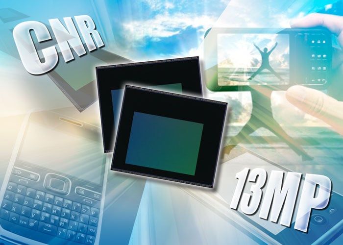
SAN JOSE, Calif., — Toshiba America Electronic Components, Inc. (TAEC)*, a committed leader that collaborates with technology companies to create breakthrough designs, announced a new 13 mega pixel, 1.12 micrometer, CMOS image sensor delivering high-image quality equivalent to a 1.4 micrometer pixel image sensor. Toshiba implemented back side illumination (BSI) technology and integrated color noise reduction (CNR) to develop its newest CMOS image sensor that fits into an 8.5mm x 8.5mm size camera module and enables high-quality pictures even in low-light conditions.
"As mobile devices like smartphones and tablets get smaller and thinner, the pixel size of image sensors needs to shrink accordingly," said Andrew Burt, vice president of the Analog and Imaging Business Unit, System LSI Group at TAEC. "However, the miniaturization of pixel size reduces the amount of light entering into the pixel which impacts image quality. Toshiba addresses the challenge of pixel miniaturization with its newest CMOS image sensor."
The miniaturization of pixel size impacts performance of light sensitivity and signal to noise ratio (SNR) in today's 1.12 micrometer pixel image sensors. BSI technology helps improve sensitivity, but falls short on elevating image quality. Leveraging its innovation and technology expertise, Toshiba developed its newest CMOS image sensor with BSI and CNR integrated on the sensor to address both low-light sensitivity and SNR. As a result, the Toshiba CMOS image sensor provides approximately 1 ½ times higher SNR value1 than a 1.12 micrometer pixel image sensor with no CNR feature allowing manufacturers to deliver products with high-quality imagery, even in low-light conditions.
![]() Pricing and Availability
Pricing and Availability
Samples of the Toshiba 13 mega pixel, 1.12 micrometer CMOS image sensor, part number T4K37, will be available in December 2012 . Sample pricing begins at $ 20.00 (U.S.). For more information go to: http://www.toshiba.com/taec/adinfo/cmos/
*About TAEC
Through proven commitment, lasting relationships and advanced, reliable electronic components, Toshiba enables its customers to create market-leading designs. Toshiba is the heartbeat within product breakthroughs from OEMs, ODMs, CMs, VARs, distributors and fabless chip companies worldwide. A committed electronic components leader, Toshiba designs and manufactures high-quality flash memory-based storage solutions, solid state drives (SSDs ), hard disk drives (HDDs), discrete devices, advanced materials, medical tubes, custom SoCs/ASICs, imaging products, microcontrollers and wireless components that make possible today's leading smartphones, tablets, MP3 players, cameras, medical devices, automotive electronics, enterprise solutions and more.
Toshiba America Electronic Components, Inc. is an independent operating company owned by Toshiba America, Inc., a subsidiary of Toshiba Corporation, Japan 's largest semiconductor manufacturer and the world's third largest semiconductor manufacturer (Gartner, 2011 Worldwide Semiconductor Revenue, March 2012). Toshiba Corporation was founded in 1875 and today has over 554 subsidiaries and affiliates, with 210,000 employees worldwide. Visit Toshiba's web site at www.toshiba.co.jp/index.htm.
1Based upon Toshiba measurements
Information in this press release, including product pricing and specifications, content of services and contact information, is current and believed to be accurate on the date of the announcement, but is subject to change without prior notice. Technical and application information contained here is subject to the most recent applicable Toshiba product specifications. In developing designs, please ensure that Toshiba products are used within specified operating ranges as set forth in the most recent Toshiba product specifications and the information set forth in Toshiba's "Handling Guide for Semiconductor Devices," or "Toshiba Semiconductor Reliability Handbook." This information is available at www.toshiba.com/taec, or from your TAEC representative.
Editors Note: Reader inquiries please publish: Tech.Questions@taec.toshiba.com. Photos available for download at Photo Gallery
Image: http://www.toshiba.com/taec/news/images/gallery/imaging/T4K37_lrg.jpg
ASSP 12 654