
September 23, 2020
TOKYO--Toshiba Electronic Devices & Storage Corporation (“Toshiba”) and its manufacturing subsidiary, Japan Semiconductor Corporation, have developed Laterally Double Diffused MOS (LDMOS) cell array design that is highly tolerant of negative carrier injection and electrostatic discharge (ESD) events. Compared to a reference structure the new design is 40% more tolerant of allowable negative injection current. [1]
Details of the achievement were reported at the IEEE-sponsored International Symposium on Power Semiconductor Devices and ICs 2020 (ISPSD 2020), held online.
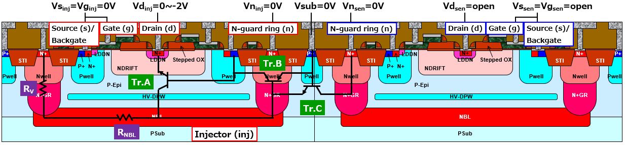
Analog ICs are essential for various consumer electronics, industrial equipment and automotive equipment. LDMOS installed in Analog ICs must be highly reliable, and tolerance of negative carrier injection is an important characteristic. When negative carriers are injected into the switching device (injector) drain, a parasitic bipolar transistor is turned on and minority carriers are injected into the substrate. This has an undesirable influence on surrounding devices. Tolerance of ESD events, static electricity that results in damage or malfunction, is also required. To improve tolerance against a negative carrier injection and ESD events, devices are separate by distance or an N-guard ring is inserted between devices, but both approaches increase chip size and production costs.
Toshiba and Japan Semiconductor focused on the fact that tolerance of negative carrier injection is higher when resistance in the N-guard ring in the injector is small, and investigated tolerance of negative carrier injection and ESD events in multiple LDMOS array designs.
The companies found positive correlation between a parameter obtained by dividing the width of the N-guard ring area by the maximum area of the divided array and tolerance of negative carrier injection. They also found a negative correlation between the parameter and tolerance of ESD events. This indicates a tradeoff between tolerance of negative carrier injection and of ESD events. This tradeoff showed the companies that design No.10 has the best layout, as it increased negative injection current by 40% against a reference structure, degradation of tolerance of ESD events was suppressed to only 9%, and the total area increase was kept to less than 15%. [1]
The companies can apply the new technology to fourth generation LDMOS, which entered mass production in 2019.
Toshiba has a wide lineup of LDMOS for various voltages and applications, and is developing fifth generation LDMOS. This will integrate embedded non-volatile memory (eNVM) and high voltage analog ICs.
Toshiba Electronic Devices & Storage Corporation and Japan Semiconductor Corporation are committed to semiconductor process R&D that contributes to low power consumption and minimized equipment size.
Cross-sectional view of Nch-LDMOS
Measured LDMOS structures (3600 cell)
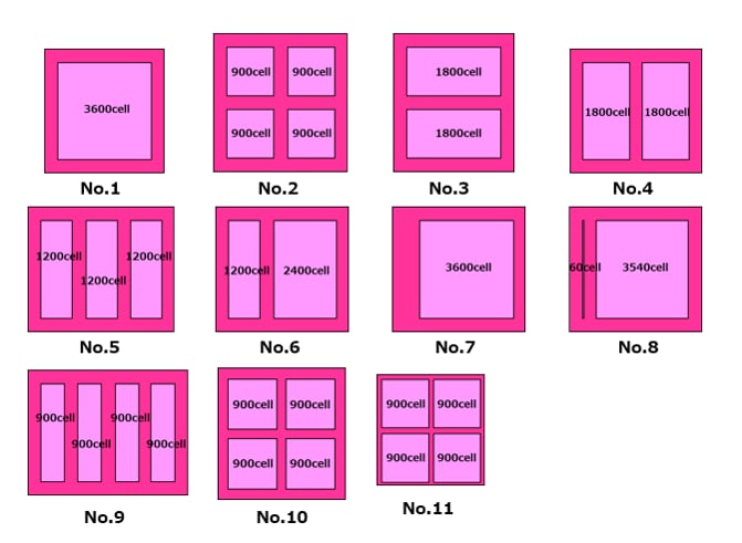
Dark pink area indicates N-guard ring, and light pink area indicates internal cell.
Relationship between tolerance of negative carrier injection and ESD events on total area ratio
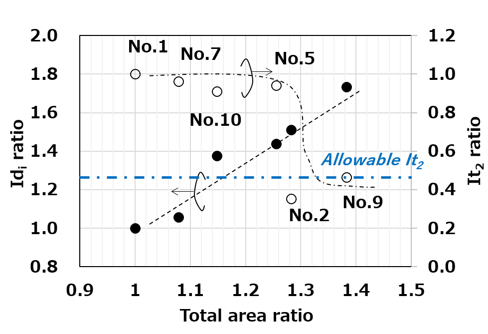
Idi: Tolerance of negative carrier injection
It2: Tolerance of ESD events
Both values are normalized by the value of No.1 as a reference.
Notes:
[1] Comparison of tolerance against negative carrier injection in the best structure (No.10) and the reference structure (No.1).
Information in this press release, including product pricing and specifications, content of services and contact information, is current and believed to be accurate on the date of the announcement, but is subject to change without prior notice. Technical and application information contained here is subject to the most recent applicable Toshiba product specifications.