Toshiba Succeeds in Reducing On-resistance in SBD embedded SiC MOSFET While Securing Reliability and Short-Circuit Ruggedness
June 3, 2024
Toshiba Electronic Devices & Storage Corporation
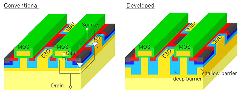
Kawasaki, Japan-Toshiba Electronic Devices & Storage Corporation (“Toshiba”) has developed a Schottky barrier diode (SBD)[1] embedded metal oxide semiconductor field effect transistor (MOSFET)[2], a significant improvement over the current device structure[3], while maintaining high reliability and short-circuit ruggedness. A successful design modification introduces a barrier structure[4] with varying depths in the device structure that maintains the reliability of the reverse conduction operation[5], the function of an integrated SBD, while suppressing the current leakage from the SBD part that causes destruction during short-circuiting[6]. By making use of new design technology and optimizing the device structure, the new MOSFET achieves lower on-resistance[7] (RonA), with about a 26% improvement over the current structure[3].
Power semiconductors play a central role in electricity supply and control. They cut energy consumption in all kinds of electronic equipment, and are an important tool for the realization of carbon neutrality. Continued demand expansion is expected from vehicle electrification and the miniaturization of industrial equipment. Against this background, SiC MOSFETs are seen as next-generation power semiconductors. They deliver better power energy conversion efficiency than Si MOSFETs, and their use has expanded rapidly in recent years. However, SiC MOSFETs have a reliability problem: increased RonA due to reverse conduction operation. Toshiba has now developed an SBD-embedded SiC MOSFET that operates in reverse conduction without increasing RonA.
Reducing the RonA of SiC MOSFET simultaneously causes excess current flow through the MOSFET part during short-circuit operation[6], reducing the durability of short-circuit operation. However, enhancing the conduction of the embedded SBD to improve the reliability of reverse conduction operation increases its current leakage during short-circuit operation, which also decreases the durability of short-circuit operation. Introducing a deep barrier structure can suppress both the excess current of the MOSFET and SBD current leakage during short-circuit operation, but it also obstructs current flow from the SBD, raising concerns about decreased reliability in diode conduction.
This led Toshiba to consider a barrier structure divided into shallow and deep areas. The deep barrier area successfully suppresses excess current from the MOSFET part during short-circuit operation, and reduces SBD current leakage, while leaving a shallow area effectively spreads current from the SBD without any obstruction by the barrier. This improves ruggedness during short-circuit operation while maintaining excellent reliability in reverse conduction operation. Toshiba has provided some customers with test samples of SiC MOSFETs with embedded SBD that apply the new technology since December 2023 for evaluation, toward further enhancing performance.
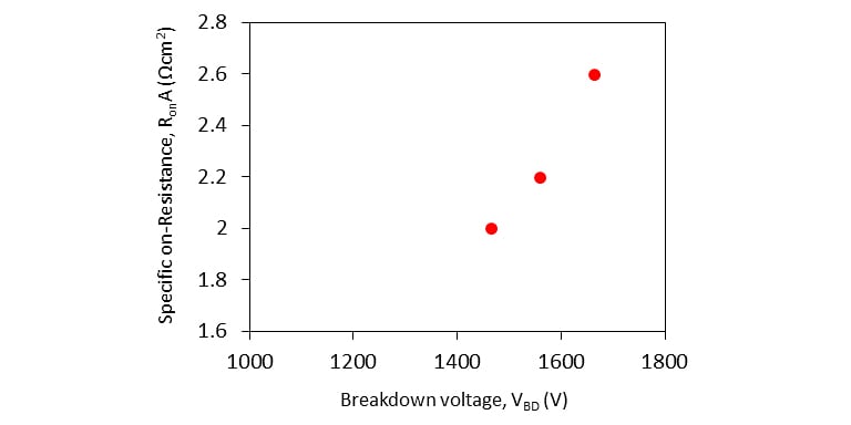
By making use of its new design technology and optimizing the device structure, Toshiba has developed a prototype 1.2 kV class SBD-integrated MOSFET. This achieves a low RonA of 2.0 mΩcm2, about a 26% improvement over the current structure[3] (Figure 2). Toshiba will present the details of this technology on June 3 (local time) at The 36th International Symposium on Power Semiconductor Devices and ICs (ISPSD) 2024, an international conference on power semiconductors, which is being held in Bremen, Germany from June 2 to 6.
[1] SBD: Schottky Barrier Diode, a rectifying element that aligns the flow of current in one direction, connected within a single crystal of metal and n-type semiconductor.
[2] MOSFET: Metal Oxide Semiconductor Field Effect Transistor, it is a switching element that has three electrodes: gate, drain, and source. By applying gate voltage, it switches the on-off current between the drain and source.
[3] The device structure with SBD distribution with checkerboard-pattern, announced on December 9, 2022.
Toshiba Develops SiC MOSFET with Embedded Schottky Barrier Diode that Delivers Low On-Resistance and High Reliability
[4] Barrier Structure: An element of the device structure provided to control the high electric field due to high voltage. It greatly affects the performance of the device.
[5] Reverse Conduction Operation: An operation in which current flows from the source to the drain of the MOSFET due to the reflux of current in the circuit.
[6] Short-Circuit Operation: A phenomenon where long-term conduction occurs during abnormal mode such as control circuit failures, compared to short-term conduction during normal switching operation. Ruggedness that does not fail with a certain duration of short-circuit operation is required.
[7] On-resistance is the resistance value between the drain and source of a MOSFET during operation (ON)


* Company names, product names, and service names may be trademarks of their respective companies.
Information in this press release, including product pricing and specifications, content of services and contact information, is current and believed to be accurate on the date of the announcement, but is subject to change without prior notice. Technical and application information contained here is subject to the most recent applicable Toshiba product specifications.