Toshiba Is Sampling an Automotive CXPI Responder Interface IC that Contributes to Shorter Software Development Times
September 3, 2024
Toshiba Electronic Devices & Storage Corporation

KAWASAKI, Japan–Toshiba Electronic Devices & Storage Corporation ("Toshiba") has today started to provide samples of “TB9033FTG,” an automotive Clock Extension Peripheral Interface[2] (CXPI) responder interface IC that conforms to the CXPI standard for automotive communications protocols.
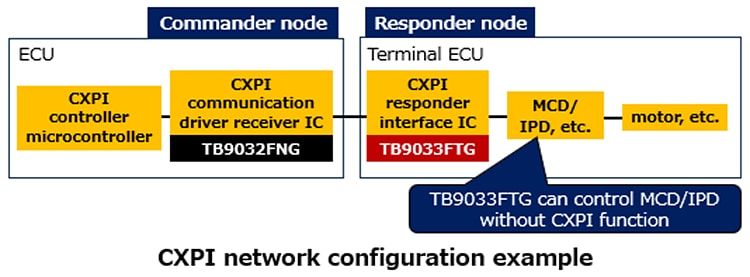
TB9033FTG is the industry’s first[1] IC of its type with built-in hardware logics[3], which control transmission and reception by the CXPI protocol and general purpose input/output (GPIO). This eliminates the need for development of dedicated software and contributes to shorter product development times.
The new IC has 16 GPIO pins. Six can be switched to AD converter input, and four to pulse width modulation (PWM) output. It also integrates functions that allow use in a broad spectrum of automotive applications: input monitoring during Sleep Mode; switch matrix (max 4×4) input; and output in the event of communications disruption.
Fault detection circuits for overheat, overvoltage and low voltage are built into the IC. It also can detect conditions that precede an abnormality and send the data to the commander node, improving fault detection performance in automotive applications.
The operating temperature range is from -40 to 125°C which is suitable for automotive applications, and the IC will conform to the AEC-Q100 qualification standard for automotive electronics.
The new product’s support for multiplexing automotive communications and reducing the number of wire harnesses used in body control systems will contribute to lower vehicle weight.
Toshiba is also developing an automotive CXPI communications driver receiver IC “TB9032FNG” that can be switched between commander node and responder node via an external pin.
Notes:
[1] As CXPI interface IC for responder nodes. As of September 3, 2024, Toshiba survey.
[2] CXPI (Clock Extension Peripheral Interface): A communications standard, developed in Japan for automotive sub-networks derived from LIN[4].
[3] Logic circuits configured with hardware without a microcontroller
[4] LIN (Local Interconnect Network): A communications standard for lower-cost, lower-speed on-board subnetworks than provided by CAN[5]
[5] CAN (Controller Area Network): A serial communications standard, primarily used for automotive communications networks.

Applications
Automotive
- Body control system applications (steering wheel switches, meter cluster switches, light switches, door locks, door mirrors, etc.)
Features
- Responder interface IC conforming to the CXPI standard for automotive communications protocols
- High-speed response suitable for automotive body system applications (compared with LIN)
- 16 GPIO pins (four can be switched to PWM output, another six can be converted to AD converter input)
- Switch matrix (max 4×4) input function
- Fault detection functions (This product can detect conditions that precede an abnormality and automatically send the data to the commander node.): Overheat, overvoltage and low voltage
- Low current consumption (Standby Current): IVBAT_SLP=10μA (typ.)
- Low EMI and high EMS make noise design easier
- Highly resistant to static electricity due to its high ESD resistance
- To be AEC-Q100 qualified
Main Specifications
(Ta=-40 to 125°C)
| Part number | TB9033FTG | ||
|---|---|---|---|
| Standard | Conforming to CXPI (ISO 20794-2 to 4, ISO 14229-8) of the standard for automotive communications protocols | ||
| Functions | CXPI interface IC with built-in hardware logics (responder node only) | ||
| I/O pins | 16 GPIO pins (4.5 to 5.5V) (six pins can be switched to one circuit of 10bit AD converter input and four pins can be switched to four circuits of 8bit PWM output.) |
||
| Input functions |
|
||
| Output functions |
|
||
| Built-in memory | Non-volatile memory (saving I/O pin settings, rewriteable and passwords configurable) | ||
| Fault detection functions | Overheat, overvoltage and low voltage (This product can detect conditions that precede an abnormality and automatically send the data to the commander node.) | ||
| Absolute maximum ratings |
Power supply voltage VVBAT (V) |
-0.3 to 40 | |
| Electrical characteristics |
VBAT normal operating range VVBAT (V) |
6 to 18 | |
| Current consumption (Standby Current) IVBAT_SLP (μA) |
Typ. | 10 | |
| Operating temperature Ta (°C) |
-40 to 125 | ||
| Communication speed (kbps) | Max | 20 | |
| Package | Name | P-VQFN28-0606-0.65-003 | |
| Size (mm) | 6×6 | ||
| Reliability test | To be AEC-Q100 (Grade1) qualified | ||
| Mass production | December 2025 | ||
Follow the link below for more on the new product.
Follow the link below for more on Toshiba’s products for automotive network communications.
Customer Inquiries:
Analog & Automotive Device Sales & Marketing Dept.
Tel: +81-44-548-2219
* Company names, product names, and service names may be trademarks of their respective companies.
Information in this press release, including product pricing and specifications, content of services and contact information, is current and believed to be accurate on the date of the announcement, but is subject to change without prior notice. Technical and application information contained here is subject to the most recent applicable Toshiba product specifications.