


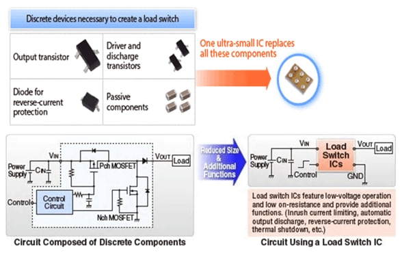
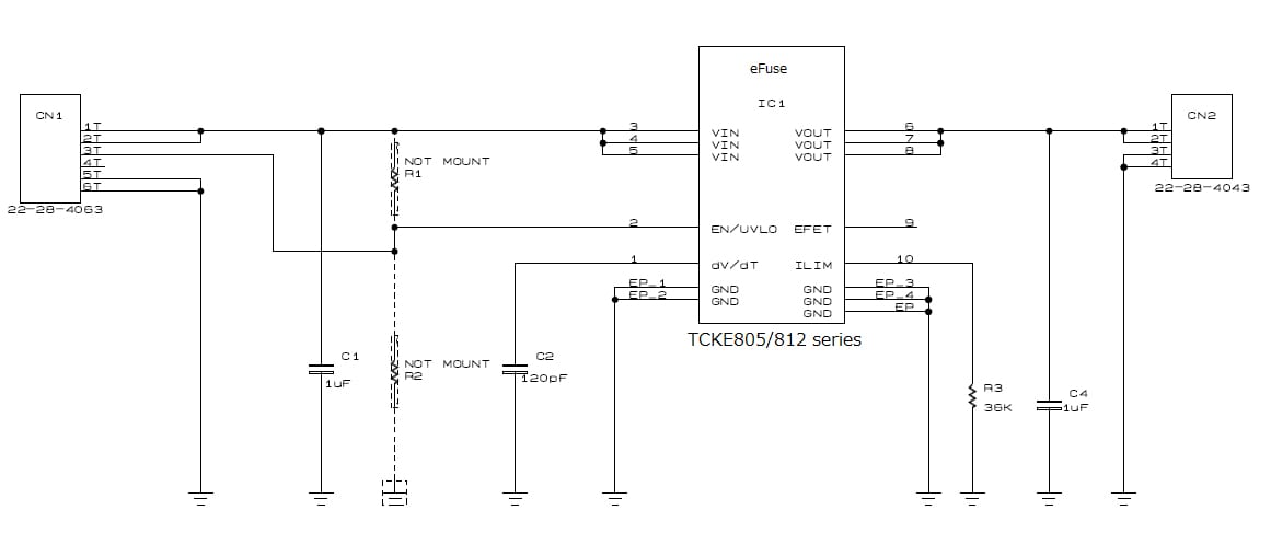
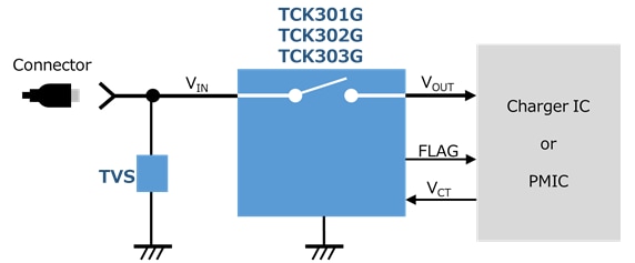
Load Switch ICs
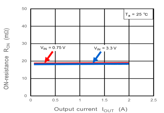
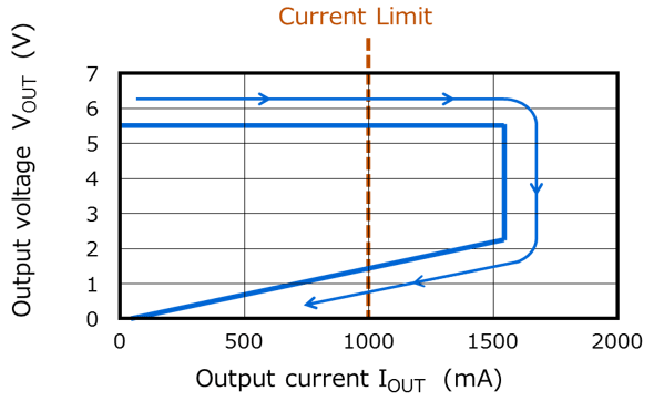
The load switch IC is a power supply IC fabricated using CMOS processes and featuring built-in output transistors and output drivers. Compared with the conventional discrete configuration, this system is greatly reduced in size. It also features low-voltage operation, low-on-resistance characteristics, and low current consumption, and is equipped with various additional functions. The package lineup focuses on ultra-small products of the 1 mm2 class. In particular, the package lineup provides products that are suitable for use in portable devices that require space saving.
Lineup
You can narrow down the search for applicable products by selecting specifications.
You can narrow down your search for applicable products by package type or number of pins.

- WCSP4G
-
Package Size
W : 0.645 mm 0.025 inch L : 0.645 mm 0.025 inch H : 0.465 mm 0.018 inch

- WCSP4D
-
Package Size
W : 0.79 mm 0.031 inch L : 0.79 mm 0.031 inch H : 0.55 mm 0.022 inch

- WCSP4C
-
Package Size
W : 0.9 mm 0.035 inch L : 0.9 mm 0.035 inch H : 0.5 mm 0.020 inch

- DFN4A
-
Package Size
W : 1.2 mm 0.047 inch L : 1.2 mm 0.047 inch H : 0.38 mm 0.015 inch
- SOT-25 (SMV)
-
Package Size
W : 2.9 mm 0.11 inch L : 2.8 mm 0.11 inch H : 1.1 mm 0.043 inch

- WCSP6E
-
Package Size
W : 1.2 mm 0.047 inch L : 0.8 mm 0.031 inch H : 0.55 mm 0.022 inch

- WCSP6G
-
Package Size
W : 1.2 mm 0.047 inch L : 0.8 mm 0.031 inch H : 0.35 mm 0.014 inch

- WCSP6C
-
Package Size
W : 1.5 mm 0.059 inch L : 1.0 mm 0.039 inch H : 0.5 mm 0.020 inch

- WCSP9
-
Package Size
W : 1.5 mm 0.059 inch L : 1.5 mm 0.059 inch H : 0.54 mm 0.021 inch

- WCSP16C
-
Package Size
W : 1.9 mm 0.075 inch L : 1.9 mm 0.075 inch H : 0.54 mm 0.021 inch
All package dimensions are guaranteed in millimeters as mentioned on datasheet. Package dimension in inches is round to 2 significant digits converted with 1mm=0.0393701inch.
require 3 characters or more.
About information presented in this cross reference
The information presented in this cross reference is based on TOSHIBA's selection criteria and should be treated as a suggestion only. Please carefully review the latest versions of all relevant information on the TOSHIBA products, including without limitation data sheets and validate all operating parameters of the TOSHIBA products to ensure that the suggested TOSHIBA products are truly compatible with your design and application.Please note that this cross reference is based on TOSHIBA's estimate of compatibility with other manufacturers' products, based on other manufacturers' published data, at the time the data was collected.TOSHIBA is not responsible for any incorrect or incomplete information. Information is subject to change at any time without notice.
Technical Articles


Documents
Technical topics
Applications
Reference Design


Queries about purchasing, sampling and IC reliability
Stock Check & Purchase
require 3 characters or more.