Load Switch ICs (負載開關 ICs)

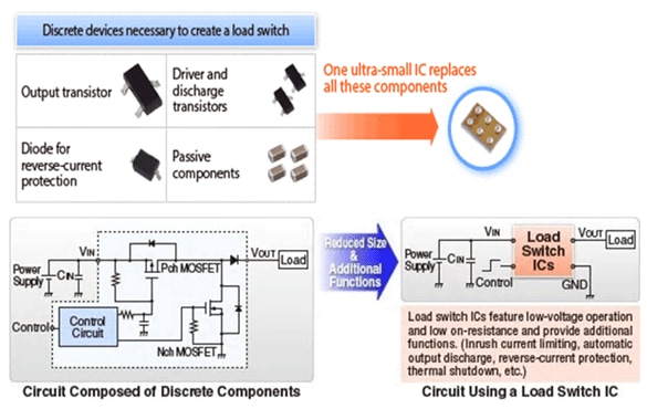
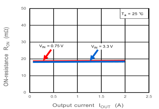
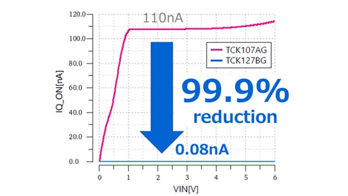
負載開關IC是使用CMOS製程的電源IC,並內建輸出電晶體和輸出驅動器。與傳統的離散配置相比,該系統的尺寸大大減小。它還具有低壓工作,低導通電阻特性和低電流消耗的特點,並配備了各種附加功能。包裝產品系列集中於1 mm2級的超小型產品。特別地,包裝陣容提供適合在需要節省空間的攜帶式設備產品。

產品陣容

You can narrow down the search for applicable products by selecting specifications.

Operating input voltage VIN (Min) (V)
Operating input voltage VIN (Max) (V)
Maximum Output Current (DC) IOUT (DC) (Max) (A)
-
Function
Protection
Width×Length×Height
Results:

You can narrow down your search for applicable products by package type or number of pins.

unit:

All package dimensions are guaranteed in millimeters as mentioned on datasheet. Package dimension in inches is round to 2 significant digits converted with 1mm=0.0393701inch.

About information presented in this cross reference

The information presented in this cross reference is based on TOSHIBA's selection criteria and should be treated as a suggestion only. Please carefully review the latest versions of all relevant information on the TOSHIBA products, including without limitation data sheets and validate all operating parameters of the TOSHIBA products to ensure that the suggested TOSHIBA products are truly compatible with your design and application.
Please note that this cross reference is based on TOSHIBA's estimate of compatibility with other manufacturers' products, based on other manufacturers' published data, at the time the data was collected.
TOSHIBA is not responsible for any incorrect or incomplete information. Information is subject to change at any time without notice.

Smaller Area and Higher Functionality
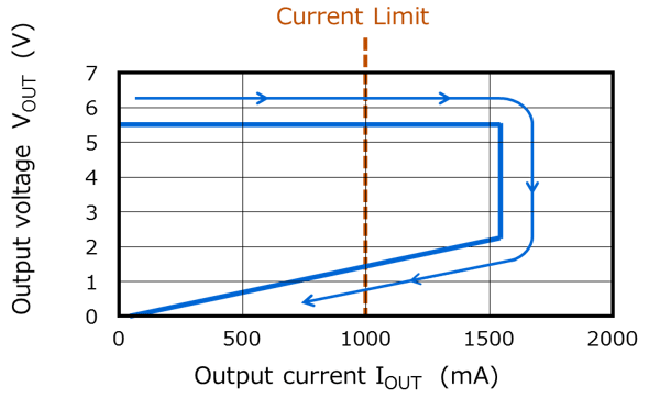
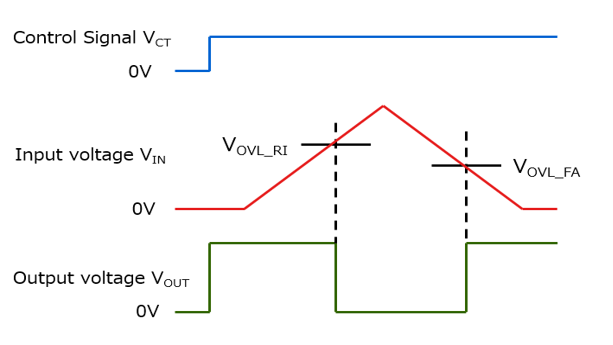
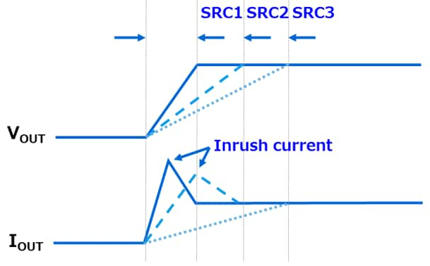
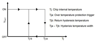
東芝負載開關IC具有多種附加功能,這些功能與配置有分立組件的常規電路配置相複雜,例如,單芯片IC中的湧入電流降低,反向電流阻斷,過流保護,熱關斷和自動輸出放電等。他們輕鬆實現了小面積,低成本的高性能係統。
Discrete devices necessary to create a load switch

文件下載

名稱 日期

技術議題

應用

Solid State Drive
Such as low power consumption and miniaturization are important in designing solid state drive (SSD). Toshiba provides information on a wide range of semiconductor products suitable for power supply/power supply management units, surge/ESD protection circuit units, over temperature monitoring unit, etc., along with circuit configuration examples.
Wireless Charger
Such as low power consumption and miniaturization are important in designing wireless charger. Toshiba provides information on a wide range of semiconductor products suitable for power supply unit, inverter circuit unit, etc., along with circuit configuration examples.

參考設計

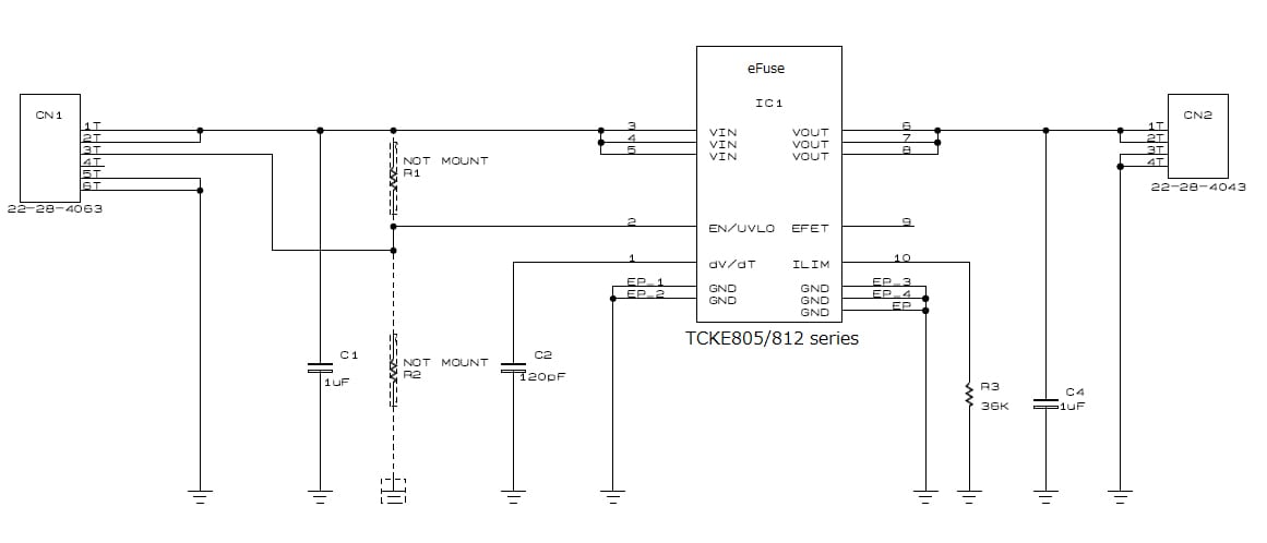
Circuit of application circuits of eFuse IC TCKE805 series.
Application Circuits of eFuse IC TCKE805 Series
Power line protection circuit with TCKE805 series. It achieves rapid shutdown at short circuit, other protection functions, and anti back current circuit with an external MOSFET.
eFuse / TCKE805
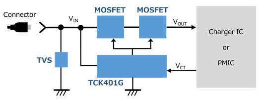
Battery charger circuit of MOSFET Driver IC application and circuit of the TCK401G.
MOSFET Driver IC Application and Circuit of the TCK401G
This reference design provides technical information on slew rate control, auto discharge and other built-in functions for designing load switch circuit suitable for USB-PD.
Semiconductor / power supply / power management / topology / flyback / AC-DC / MOSFET / diode
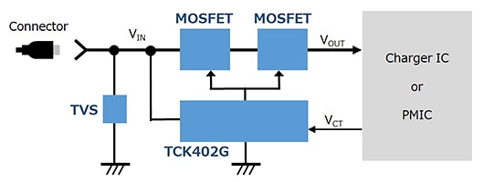
Battery charger circuit of MOSFET Driver IC application and circuit of the TCK402G.
MOSFET Driver IC Application and Circuit of the TCK402G
This reference design provides technical information on slew rate control, auto discharge and other built-in functions for designing load switch circuit suitable for USB-PD.
Semiconductor / power supply / power management / topology / flyback / AC-DC / MOSFET / diode
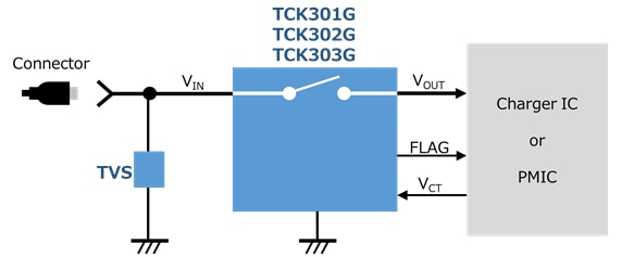
Main switch of a rapid-charging circuit of load switch IC TCK301G, TCK302G, TCK303G application & circuit.
Load Switch IC TCK301G, TCK302G, TCK303G Application & Circuit
This reference design provides example circuit of the load switch with low on resistance and built-in in-rush current control function. It is suitable for battery used application.
Load Switch IC / Application & Circuit
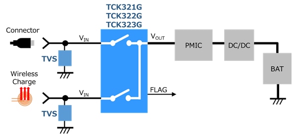
Battery charger circuit of load switch IC TCK321G, TCK322G, TCK323G application & circuit.
Load Switch IC TCK321G, TCK322G, TCK323G Application & Circuit
This reference design provides document with input selection characteristics. The load switch has small package and low on resistance suitable for battery charging application.
Load Switch IC / Application & Circuit / Design / Support / Reference Design Center

聯繫我們

技術方面問題

聯絡我們

聯絡我們

常見問題

常見問答

採購 / 樣品 / IC可靠度 相關問題

線上庫存查詢跟購買

keyword:

Disclaimer for External Link
Through this website you are able to proceed to the website of our distributors ("Third Party Website") which is not under the control of Toshiba Corporation and its subsidiaries and affiliates (collectively "Toshiba"). The Third Party Website is made available to you as a convenience only and you agree to use the Third Party Website at your own risk. The link of the Third Party Website does not necessarily imply a recommendation or an endorsement by Toshiba of the Third Party Website. Please be aware that Toshiba is not responsible for any transaction done through the Third Party Website, and such transactions shall be subject to terms and conditions which may be provided in the Third Party Website.
開啟新視窗