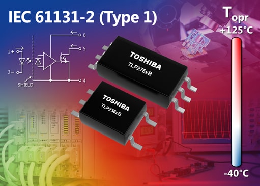
Diodes

Toshiba offers an extensive portfolio of diodes, including high-speed, low-loss Schottky-barrier diodes (SBDs) and TVS diodes (ESD protection diodes ) for high-speed signal lines.
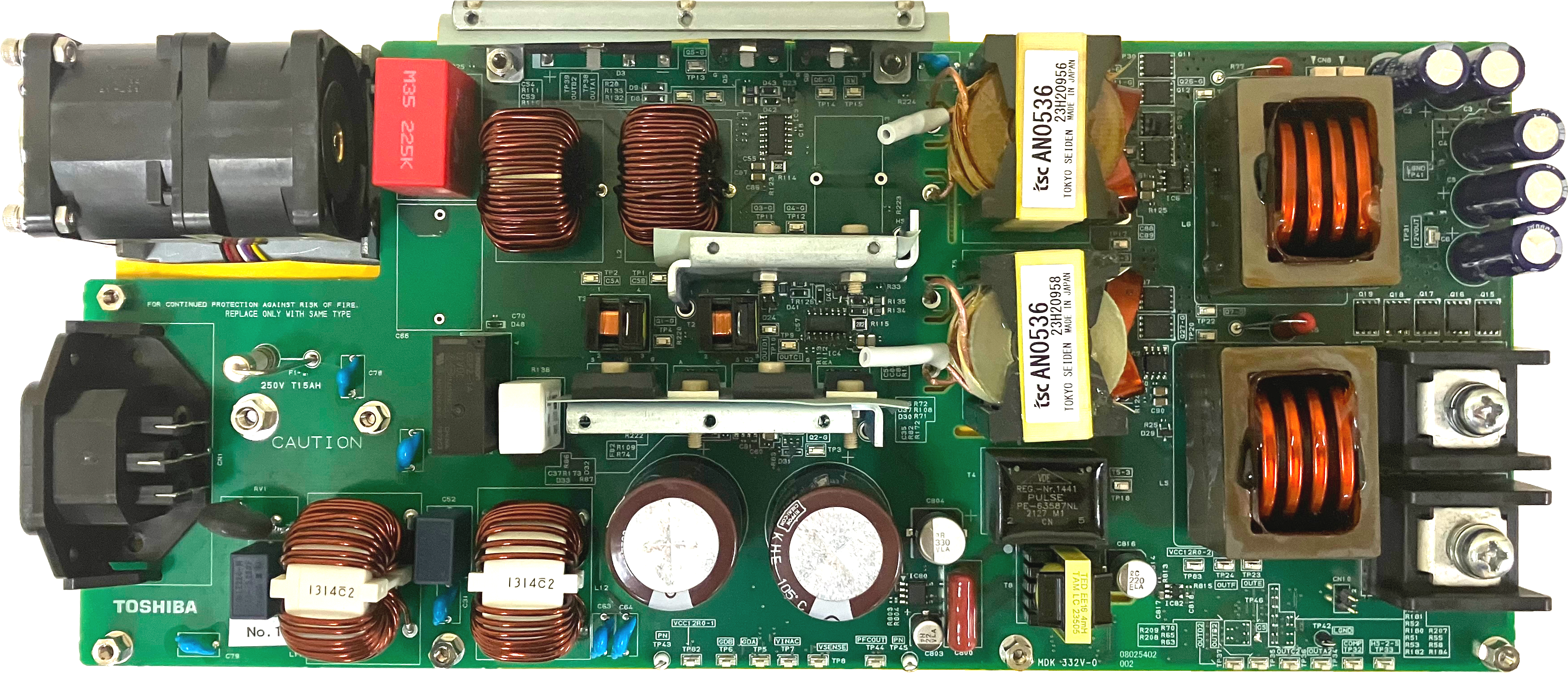
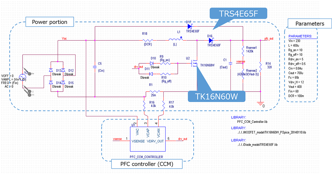
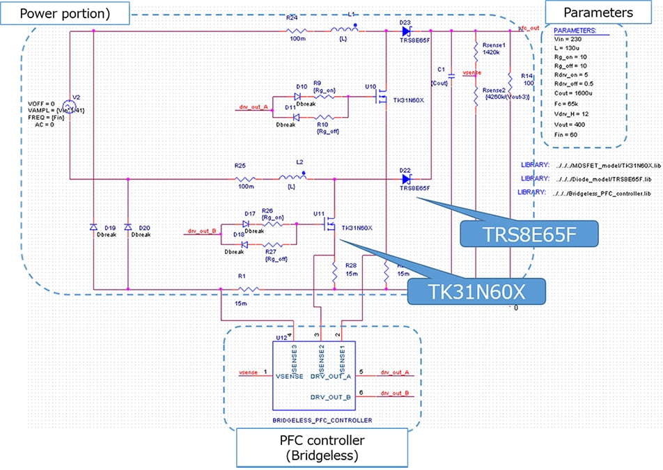
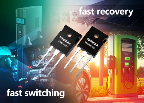
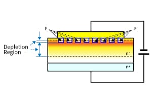
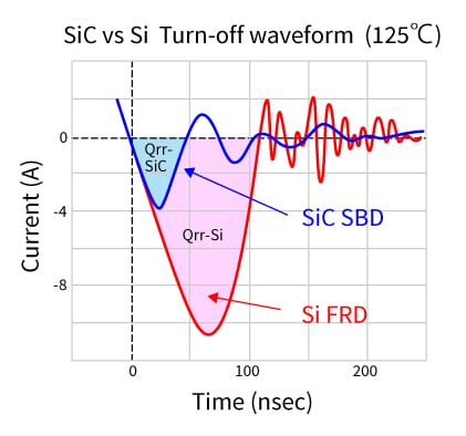
Fabricated using silicon carbide (SiC), SiC SBDs provide high breakdown voltage that has never been possible with silicon (Si) SBDs. SiC SBDs are ideal for low-loss, high-efficiency power conversion applications such as server power supplies and solar power conditioners.

Lineup

TVS Diodes (ESD Protection Diodes)
Toshiba offers ESD protection diodes in small packages for protecting various interfaces. Fabricated with unique process technology, our TVS diodes provide high ESD tolerance.
SiC Schottky Barrier Diodes
Toshiba offers 650-V silicon carbide Schottky barrier diodes (SiC SBDs) with a rated current of 2 A to 10 A.
Schottky Barrier Diodes
Toshiba offers superior low-VF and low-IR types ranging from general-purpose to power-line products. These can contribute to greater power efficiency and power saving.
Automotive Diodes
Toshiba has developed an abundant lineup of suitably small and efficient products, such as TVS diodes, rectifiers, Zener diodes, and Schottky barrier diodes, in small and medium-size surface-mount packages.
Rectifier Diodes
Diodes with reverse voltage ranging from 200 to 1000 V and an average forward current ranging from 0.5 to 3 A are offered in small and medium-size surface-mount packages.
Switching Diodes
Toshiba offers 1-circuit to 4-circuit products, with forward current ranging from 80 to 500 mA, in small surface-mount packages suitable for high-density board assembly.
Zener Diodes
Zener diodes are available in a wide range of Zener voltage specifications extending from 5.6 V to 82 V. Their extensive application fields include both consumer and industrial electronics.
RF Diodes
Toshiba offers variable capacitance diodes, PIN diodes, switch diodes, and Schottky barrier diodes for high-frequency matching circuits, band switching, RF detection circuits, mixer circuits, etc.

Cross Reference Search

About information presented in this cross reference

The information presented in this cross reference is based on TOSHIBA's selection criteria and should be treated as a suggestion only. Please carefully review the latest versions of all relevant information on the TOSHIBA products, including without limitation data sheets and validate all operating parameters of the TOSHIBA products to ensure that the suggested TOSHIBA products are truly compatible with your design and application.
Please note that this cross reference is based on TOSHIBA's estimate of compatibility with other manufacturers' products, based on other manufacturers' published data, at the time the data was collected.
TOSHIBA is not responsible for any incorrect or incomplete information. Information is subject to change at any time without notice.

Documents

Name Date

Technical topics

Reference Design

PCB Photo (example)
1.6 kW Server Power Supply (Upgraded)
Thanks to Toshiba’s latest power devices and digital isolator, this 1U size and 12 V output 1.6 kW server power supply achieves higher efficiency at whole load than the existing reference design which uses the same circuit topology. Design files and guides for circuit design and operation are available as reference design.
PCB photo example of Power multiplexer circuit
Power Multiplexer Circuit Using Common-Drain MOSFET
This power multiplexer circuit with 2 inputs and 1 output is realized on a small board. A new power multiplexer circuit usign common-drain MOSFET has been added to the already developed power multiplexer circuit reference design. These reference circuits allow switching between BBM and MBB modes by combining optimal devices such as MOSFET gate driver ICs and zener diodes from our diverse product lineup.
Power multiplexer circuit / 2 input and 1 output
PCB Photo (example)
Application Circuit of Low Power Consumption Op-Amp TC75S102F
Application circuits of low power consumption Op-Amp TC75S102F for use with various sensors. These application circuits can be used for devices requiring long battery life, IoT sensor, energy harvesting, etc.
1.6 kW T-Type 3-Level PFC Power Supply
This reference design provides design guide, data and other contents of 1.6kW AC-DC converter power supply using T-Type 3-Level power factor correction (PFC) circuit.
PCB photo example of Power multiplexer circuit
Power multiplexer circuit
In this reference design, a Power multiplexer circuit with 2 input and 1 output is implemented on a small PCB. MOSFET gate driver ICs, eFuse ICs, zener diodes and small package MOSFETs selected from Toshiba's diverse lineup are used create ideal diode like characteristics with BBM and MBB switching.
Power multiplexer circuit / 2 input and 1 output
Features of 1.2V/100A output DC-DC converter compliant with 48V bus voltage.
1.2V/100A Output DC-DC Converter Compliant with 48V Bus Voltage
This reference design provides specification, block diagram and PCB layout data of 1.2V/100A output isolated DC-DC converter which convert 48V bus voltage to 1.2V directly.
DC-DC / MOSFET / reference design
Features of 300W Isolated DC-DC converter.
300W Isolated DC-DC Converter
This reference design provides specification, block diagram and PCB layout data of 300W isolated DC-DC converter which is small size and suitable for consumer applications.
DC-DC Converter / Design / Support / Reference Design Center
Circuit diagram of single phase PFC power supply basic simulation circuit.
Single Phase PFC Power Supply Basic Simulation Circuit
This reference design provides OrCAD® based simulation circuit, simulation results and design guide. This is for designing single phase PFC power supply.
Single Phase PFC Power Supply Basic Simulation Circuit
Circuit diagram of interleaved PFC power supply basic simulation circuit.
Interleaved PFC Power Supply Basic Simulation Circuit
This reference design provides OrCAD® based simulation circuit, simulation results and design guide. This is for designing interleaved PFC power supply.
Interleaved PFC Power Supply Basic Simulation Circuit
Circuit diagram of bridgeless PFC power supply basic simulation circuit.
Bridgeless PFC Power Supply Basic Simulation Circuit
This reference design provides OrCAD® based simulation circuit, simulation results and design guide. This is for designing bridgeless PFC power supply.
Bridgeless PFC Power Supply Basic Simulation Circuit
Main switch of a rapid-charging circuit of load switch IC TCK301G, TCK302G, TCK303G application & circuit.
Load Switch IC TCK301G, TCK302G, TCK303G Application & Circuit
This reference design provides example circuit of the load switch with low on resistance and built-in in-rush current control function. It is suitable for battery used application.
Load Switch IC / Application & Circuit
Battery charger circuit of load switch IC TCK321G, TCK322G, TCK323G application & circuit.
Load Switch IC TCK321G, TCK322G, TCK323G Application & Circuit
This reference design provides document with input selection characteristics. The load switch has small package and low on resistance suitable for battery charging application.
Load Switch IC / Application & Circuit / Design / Support / Reference Design Center
Features of 1.6kW, 80Plus Platinum class, high efficiency server AC-DC power supply .
1.6kW, 80Plus Platinum Class, High efficiency Server AC-DC Power supply
This reference design provides design guide, data and other contents of 1.6kW 80Plus Platinum class power supply using Semi-bridgeless/Isolated phase shift full bridge.
Semiconductor / power supply / power management / topology / flyback / AC-DC / MOSFET / diode / Toshiba

Contacts

Technical inquiry

Contact us

Contact us

Frequently Asked Questions

FAQs
A new window will open